Impact of Post Deposition Annealing on Characteristics of Hf x Zr 1 - x O 2
- PDF / 451,213 Bytes
- 6 Pages / 612 x 792 pts (letter) Page_size
- 5 Downloads / 342 Views
1155-C07-05
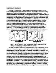
Impact of Post Deposition Annealing on Characteristics of HfxZr1-xO2 D.H. Triyoso, R.I. Hegde, R. Gregory, G.S. Spencer and W. Taylor Jr. Technology Solutions Organization, Freescale Semiconductor Inc. 3501 Ed Bluestein Blvd, Austin, TX 78721, U.S.A. ABSTRACT In this paper the impact of post deposition annealing in various ambient on electrical properties of hafnium zirconate (HfxZr1-xO2) high-k dielectrics is reported. ALD HfxZr1-xO2 films are annealed in a nitrogen and/or oxygen ambient at 500°C to 1000°C. Devices annealed at 500°C in N2 has lower equivalent oxide thickness (EOT) of 10Å without significant increase in gate leakage (Jg), threshold voltage (Vt) and only a slight decrease in transconductance (Gm) values compared to 500°C O2 annealed devices. Furthermore, the impact of annealing HfxZr1xO2 films in a reducing ambient (NH3) is studied. Optimized NH3 anneal on HfxZr1-xO2 results in lower CET, improved PBTI, low sub-threshold swing values, comparable high-field Gm with only a minor degradation in peak Gm compared to control HfxZr1-xO2. Finally, the impact of laser annealing vs. RTP annealed HfxZr1-xO2 films are reported. Laser annealing helped further stabilize tetragonal phase of HfxZr1-xO2 without inducing void formation. Good devices with low leakage, low EOT and high mobility are obtained for laser annealed HfxZr1-xO2. INTRODUCTION Hafnium based high-k dielectrics have recently been implemented by a few companies for 45nm technology node. Most companies, however, have pushed back high-k implementation until 32 nm technology node. For successful implementation at 32 nm and beyond, extending scalability of hafnium based high-k dielectrics is needed. We have recently reported stabilization of tetragonal phase of HfO2 by zirconium addition resulting in improved scalability of hafniumbased dielectrics [1-3]. This paper reports the impact of post deposition annealing in various ambient on electrical properties of hafnium zirconate high-k dielectrics.
EXPERIMENT ALD HfxZr1-xO2 films (x ~0.4) of varying thickness were annealed in a nitrogen and/or oxygen ambient at temperatures ranging from 500°C to 1000°C. All films were formed via atomic layer deposition (ALD) using hafnium tetrachloride, zirconium tetrachloride, and deuterated water at a deposition temperature of 300°C. Film thickness is controlled by the number of cycles deposited. The dielectric layer was grown on a chemical oxide starting surface. The chemical oxide was formed by cleaning Si wafers in a solution of de-ionized water, hydrogen peroxide and hydrochloric acid. For electrical characterization, the ~ 30Å high-k dielectric deposition is followed with a TaCy metal gate electrode and capped with poly-Si. The high-k dielectric films were deposited on ‘cake oxide’ wafers (wafers with 0, 50 and 100Å SiO2 in concentric rings) [3]. The NMOS long channel transistors were fabricated using conventional CMOS integration with sidewall liners and spacers, implants to the Si-cap, implants to
source/drain, 1000°C activation anneal, cobalt-sal
Data Loading...