In Situ Ellipsometric Studies of Palladium Silicide Formation
- PDF / 414,251 Bytes
- 6 Pages / 420.48 x 639 pts Page_size
- 66 Downloads / 326 Views
Mat. Res. Soc. Symp. Proc. Vol. 54. 1986 Materials Research Society
24
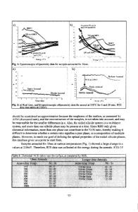
rotating - polarizer ellipsometer + uhv station
photomultiplier
double monochromator
shutter
mirrorpolarizer
analyzer lamp
•mirror
PWt•
Zaperture Ar sputter clean
--
--
C
aperture\
filament deposition
CMA
Figure 1.
Schematic of the experimental setup.
The UHV chamber, as used previously for Raman spectroscopy studies [5], is equipped with a filament deposition source for Pd, a quartz crystal thickness monitor, a cylindrical mirror analyzer Auger electron spectrometer, and argon sputter cleaning capability. The Raman window was replaced with strain-free quartz window assemblies with the appropriate angular separation for the ellipsometer. The sample stage has several translations and rotations, necessary for accurate positioning and optical alignment, and heating capability to -750 0 C. The chamber's base pressure is -5X10⁻¹⁰ Torr. The ellipsometer is in the rotating-polarizer configuration, based on a now-standard design [6] which utilizes a 75W short-arc Xenon lamp, a prism-grating double monochromator, and an end-on photomultiplier tube with extended S-20 spectral response. The polarizer and analyzer are Rochon prisms fabricated from crystal quartz and MgF 2, respectively. The mechanical rotation frequency of the polarizer is 58 Hz, and the angle of incidence was determined to be 66.54 ± 0.050. A typical spectrum consists of data recorded at 250 energies equally spaced between 1.5 and 6 eV. At each energy the complex pseudodielectric function =+i is calculated from the Fourier coefficients of the detected waveform in the two-phase (substrate-ambient) model. The sample used in these experiments was a 1X1 cm piece cut from a Sytonpolished Si wafer deliberately ~30 misoriented from . The wafer was cut from a p-type Czochralski grown single crystal with resistivity -0.1 Qcm. Organic contamination and native oxide were removed, after pumping out the UHV chamber, by Ar sputtering for several hours at 3kV and annealing at 700-750 0 C for 15 min to recrystallize the surface. The experiment consisted of several successive depositions. For annealed films the sequence was as follows: deposition, Auger, anneal, ellipsometry, Auger. For as deposited films the second and third steps were omitted. Initial depositions were 5±0.5 A, 0 with a total of 50 A of Pd. Anneals were at 300 C for 10 min. Dielectric function measurements were not made until the sample temperature, as indicated by a thermocouple on the sample holder and by an optical pyrometer, was well below 100 0 C. A few remarks are in order concerning the windows on the UHV chamber. Although the windows are nominally strain free, distortions in were observed. Even excellent window material has a residual strain birefringence, usually expressed as an optical path difference per unit thickness. An industry standard is 5 nm cm 1. But even 1 nm cm I
25
causes a phase shift in the polarization state of 1i at 4eV for a 0.25" thick quartz window. This in turn distorts the spectrum of
Data Loading...