In-Situ Heavy As Doping in Si Selective Epitaxial Growth
- PDF / 1,135,671 Bytes
- 6 Pages / 420.48 x 639 pts Page_size
- 33 Downloads / 438 Views
IN-SITU HEAVY As DOPING IN Si SELECTIVE EPITAXIAL GROWTH
Y.OHSHITA and *H.KITAJIMA Microelectronics Research Laboratories, NEC Corporation, 34 Miyukigaoka Tsukuba, Ibaraki, 305 Japan *Microelectronics Research Laboratories, NEC Corporation, 1120 Shimokuzawa Sagamihara, Kanagawa, 229 Japan ABSTRACT Role of in-situ heavy As doping in Si selective growth is studied using the SiH 2CI2/H2/HCI/AsH 3 gas system. By increasing AsH 3 flow rate, the growth rate decreases in proportion to In (AsH 3 flow rate). This result is explained well using a Frumkin-Temkin adsorption model. The As concentrations in grown films depend on surface orientation. Moreover, the maximum As concentration is about ten times lower than the solubility limit at a given temperature. These results are able to be explained qualitatively, if equilibrium concentrations of impurities at the Si(100), the Si(lll), and the bulk are assumed to be different from one another, and that the concentration at the surface is frozen in the grown film. Introduction Si selective epitaxial growth (SEG) method has been studied as one of the most important technologies for fabricating very large scale integrated circuits(VLSI) [1-1 1]. Recently, this method has been applied to contact hole refilling in metal-oxide-semiconductor (MOS) transistors, or self-aligned emitter fabrication in bipolar transistors. Due to the doping gas injection during growth, the selective growth of doped polycrystalline Si was achieved [1214]. However, when the doping gas mole fraction is comparable with the source gas amount, the growth rate decreases drastically. However, this impurity effect to the growth is not clear yet. To utilize this method in VLSI technology, the role of impurity atoms in Si SEG needs to be understood. This paper reports on studies for in-situ heavy As doping in SEG using the SiH 2Ci 2/H2/HCI/AsH 3 gas system. Experimental method
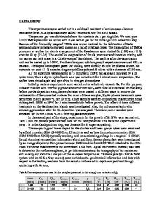
S~IR
AsH3
SiH2CI2 HOI
lamp module
H2
Fig.1 CVD apparatus blockdiagram.
ExEaust
SiH 2CI2/I-I2/HCI gas system was used for Si selective growth. The As doping was obtained by introducing arsine(AsH 3) gas during growth. The H2 carrier gas was purified through a palladium diffusion cell. An air cooled cold-wall type horizontal chemical vapor deposition (CVD) reactor with radiant heating was used for the present work. A schematic illustration of the experimental set-up is shown in Fig.1. Substrate preparation and growth procedure were as follows; Square opening were
Mat. Res. Soc. Symp. Proc. Vol. 237. 01992 Materials Research Society
572
made on 1 [trm thick field SiO2 film by conventional photolithography and successive RIE etching. Before growth, Si substrates were immersed into dilute (1%) HF solution for 30 seconds to remove the native oxide on the Si surface. Then, they were rinsed with de-ionized water. Si films were grown on Si(100) and Si(lll) substrates under reduced pressures (20 Torr total pressure). Typical growth temperature was 800 *C.The gas flow rates of SiH 2Cl2, H2, HCI, and AsH 3 were 50, 10000, 10 and 1xl0 4 - lxl1O
Data Loading...