In-Situ Rheed-Traxs Monitoring Alloy Composition of the Surface During RF-MBE Growth of GaInN and AIGaN
- PDF / 753,641 Bytes
- 6 Pages / 414.72 x 648 pts Page_size
- 90 Downloads / 286 Views
1.
*
sin(O)}
(1)
where d represents the depth from the surface where X-rays are generated, .t is the absorption coefficient of the material for X-rays, and 0 is the angle of the emitted X-ray with respect to the surface. The TRAXS signal intensity can be enhanced by setting the detector close to total reflection angle 0. Details of the RHEED-TRAXS have been published in other literature [5]. In this study, RHEED-TRAXS was applied to monitor in situ the alloy composition at the surface of nitrides by RF-MBE for the first time. 441 Mat. Res. Soc. Symp. Proc. Vol. 482 0 1998 Materials Research Society
Detector
Characteristic X-rays
Slit Be Window
Electron beam
Sample
RHEED Screen
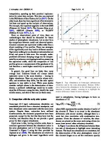
Fig.1 Schematic viewgraph of the configuration of the RHEED-TRAXS measurement system. EXPERIMENTS The nitride samples were grown on sapphire (0001) substrate by RF-MBE. Group MI sources are metallic aluminum, gallium and indium. The group V element source is nitrogen activated by a RF-plasma with a power of 300W. Growth temperature of GaN was fixed at 6501C. GainN was grown in the range of 550 to 7001C. AIGaN was grown between 650'C and 7001C. Nitrogen flow rate was kept at 1.5sccm for all layers. K-cell temperatures for metallic Ga was 970t for the growth of GaN, while that for the growth of GaInN was 9301C. In and Al K-
cell were kept at 700-C and I1OOtC, respectively. Accelerating voltage for the RHEED electron beam was 17kV. Unless otherwise noted, sampling time for the TRAXS was 30 seconds per one time. It takes about 6sec for writing the TRAXS data to the computer. The spot of the electron beam is about 1mm wide and about 4mm long. Characteristic X-rays observed in this study were GaKa (9.234keV), GaLa (1.096keV), InLa (3.287keV) and AlKc (1.487keV) lines. The detector angle was set at 1. RESULTS
Escape Depth of X-rays for GaN Escape depths of GaKa, GaLa, AlKcc InLet have measured experimentally. Fig.2(a) shows the time chart of the TRAXS signals during growth of GaN on sapphire covered with an AIN buffer layer. From this figure, escape depths of GaKa, GaLa and AIKcz through GaN are found
to be 300nm, 8nm and l5nm, respectively. Difference of the escape depth of the GaKa and GaLa was caused by the difference of the absorption coefficients of GaN for each X-ray energy. Fig.2(b) shows the time chart of the TRAXS signals for InLa during growth of GaN on thick GaInN. The escape depth was found to be 30nm.
442
1.6 1.4
-AINI
GaN
8nm
1.2
0.8
z
0.6
-
---------AlKa
1.0
Cz
GaKcc ....GaLa
..
GaN
0.4 I Nitridation
0.2
ISapphire (00011,
Sample
0.0
0
50
100
150
200
250
300
350
400
GaN thickness [nm]
(a)
1.6
1.4
S1.2 .,
1.0
,• 0.8
oaN
S0.6
GaInN
N
a
0.4
0 0.2
z
ISapphire (0001
0.0
Sample 0 50 100 150 GaInN thickness [nm]
(b)
Fig.2 Time chart of the TRAXS signals of (a) GaKa, GaLa, AIKa and (b) InLa during growth. In (a), AlKa was generated in underlying AIN through GaN. GaKa and GaLa were taken during growth of GaN. In (b), InLa was generated in the underlying GaInN through GaN. 443
A
Data Loading...