In Situ Tem Study of Reactions in Iron/amorphous Carbon Layered Thin Films
- PDF / 4,322,769 Bytes
- 6 Pages / 414.72 x 648 pts Page_size
- 102 Downloads / 293 Views
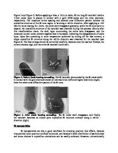
EXPERIMENTAL PROCEDURE All a-C/Fe/a-C tni-layered films were deposited using DC magnetron sputtering in a 3 rmTorr Ar atmosphere with no substrate heating. The base pressure of the system was less than 5x 10⁻⁸ Torr. Two different structures of films were prepared in this study. One is C(000lA)/Fe(200A)/C(1000A) films deposited on oxidized Si substrates which were used for cross-section TEM experiments. The other was C(200A)/Fe(100A)/C(200A) free-standing films which were used for plan-view TEM observations. The free-standing films were deposited on glass substrates coated with photo-resist and then removed from the substrate by dissolving the photo-resist with acetone. A Philips 430ST microscope operating at 300 kV, with a point resolution of around 1.9A was used in this study. Plan-view TEM samples were prepared by mounting tri-layer freestanding films on Cu grids. Cross-section TEM samples were made by a standard procedure [18]. In situ heating experiments were performed on both the plan-view and cross-section samples using a Philips single tilt heating holder. Step annealing was used in this experiment, with a step value of 50°C in the temperature range 250-600°C. The heating rate between annealing temperatures was approximately 20°C/minute. The samples were held for 30 minutes at each annealing temperature, after which pictures were taken without changing the temperature. The reliability of in-situ TEM experiments using cross-section samples was checked by comparing reactions at each temperature with those using free-standing plan-view samples since the latter are considered as "bulk" experiments. In the present study, as in previous cases [10, 11], we found good agreement between reactions in cross-section samples and those in plan-view samples. RESULTS AND DISCUSSION Figures la and lb show a bright-field (BF) image and a selected area diffraction (SAD) pattern of the as-deposited C(200A)/Fe(100A)/C(200A) tri-layered free-standing film. The SAD pattern indicates that the as-deposited film consisted of crystalline a-Fe and a-C. From a dark-field image (DF) using the a-Fe (110) diffraction ring, the grain size of Fe was measured as about 100A in diameter. A cross-section image of an as-deposited C(1000A)/Ni(200A)/C(100OA) trilayered film also revealed that the film has a well defined t'i-layered structure and that there was no reaction between the layers in the as-deposited condition (Figure 1c). No noticeable changes were observed in the film (in situ) annealed at 250°C. a
C
po
nm,
50nm
Figure 1 Plan-view (a) BF image and (b) SAD pattern of as-deposited C(200A)/Fe(100A)/C(200A) tri-layered film and (c) cross-section BF image of asdeposited C(l000A)/Fe(200A)/C(1000A) tri-layered film.
46
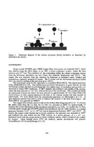
Figure 2 Plan-view (a) BF image, (b) SAD pattern and (c) DF image using Fe3C diffraction rings of C(200A)/Fe(OOA)/C(200A) tri-layered film annealed at 5000 C. Upon annealing at 300°C, some growth of the a-Fe grains was observed but the most significant change was that relatively large (about 500A in diameter) grains with "
Data Loading...