Influence of Interface States on High Temperature SiC Sensors and Electronics
- PDF / 47,890 Bytes
- 8 Pages / 612 x 792 pts (letter) Page_size
- 37 Downloads / 245 Views
K7.5.1
Influence of Interface States on High Temperature SiC Sensors and Electronics Ruby N. Ghosh1, Peter Tobias1 and Brage Golding1,2 1 Center for Sensor Materials, Michigan State Univ., East Lansing, MI 48824-2320 2 Dept. of Physics & Astronomy, Michigan State Univ., East Lansing, MI 48824-2320
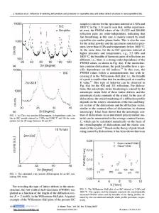
ABSTRACT Silicon carbide based metal/oxide/semiconductor (MOS) devices are well suited for operation in chemically reactive high temperature ambients. The response of catalytic gate SiC MOS sensors to hydrogen-containing species has been assumed to be due to the formation of a dipole layer at the metal/oxide interface, which gives rise to a voltage translation of the high frequency capacitance voltage (C-V) curve. From in-situ C-V spectroscopy, performed in a controlled gaseous environment, we have discovered that high temperature (800 K) exposure to hydrogen results in (i) a flat band voltage occurring at a more negative bias than in oxygen and (ii) the transition from accumulation to inversion occurring over a relatively narrow voltage range. In oxygen, this transition is broadened indicating the creation of a large number of interface states. We interpret these results as arising from two independent phenomena – a chemically induced shift in the metal/semiconductor work function difference and the passivation/creation of charged states (DIT ) at the SiO2/SiC interface. Our results are important for both chemical sensing and electronic applications. MOS capacitance gas sensors typically operate in constant capacitance mode. Since the slope of the C-V curve changes dramatically with gas exposure, we discuss how sensor-to-sensor reproducibility and device response time are influenced by the choice of operating point. For electronic applications understanding the environmentally induced changes in DIT is crucial to designing drift-free MOS devices. Our results are applicable to n-type SiC MOS devices in general, independent of the specifics of sample fabrication.
INTRODUCTION Metal/oxide/semiconductor (MOS) devices based on the wide bandgap semiconductor SiC are attractive for gas sensing and electronic device applications in harsh environments. Emissions control for both real time monitoring and feedback control of exhaust products in the automotive and energy sectors require sensors that can operate in chemically reactive high temperature environments. Turbines, automotive engines and power plants also require high temperature electronic components. The native oxide of SiC, SiO2, enables fabrication of fieldeffect devices with gate controlled modulation of the semiconductor carrier concentration. The wide bandgap of SiC allows for semiconductor device operation up to temperatures of 1200K. In addition, SiC is chemically stable in reactive environments. The performance of SiC MOS devices in these harsh, high temperature ambients will depend on the specific application as discussed below. The operation of field-effect chemical sensors are dominated by electronic and chemical interactions at interfaces. In the case of a M
Data Loading...