Influence of Post Growth Annealing on the Optical Properties of Gallium Nitride Films Grown by Pulsed Laser Deposition
- PDF / 640,975 Bytes
- 6 Pages / 432 x 648 pts Page_size
- 16 Downloads / 463 Views
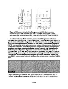
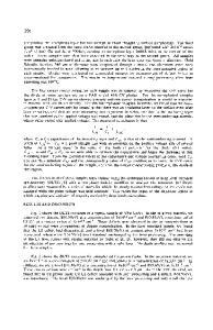
Influence of Post Growth Annealing on the Optical Properties of Gallium Nitride Films Grown by Pulsed Laser Deposition M. Baseer Haider1, M. F. Al-Kuhaili, S. M. A. Durrani, Imran Bakhtiari Department of Physics, King Fahd University of Petroleum & Minerals, Dhahran, 31261, Saudi Arabia Abstract: Gallium nitride thin films were grown by pulsed laser deposition. Subsequently, post-growth annealing of the samples was performed at 400, and 600 oC in the nitrogen atmosphere. Surface morphology of the as-grown and annealed samples was performed by atomic force microscopy, surface roughness of the films improved after annealing. Chemical analysis of the samples was performed using x-ray photon spectroscopy, stoichiometric Gallium nitride thin films were obtained for the samples annealed at 600 oC. Optical measurements of the samples were performed to investigate the effect of annealing on the band gap and optical constants the films. Keywords: GaN, PLD, nitride semiconduct ors, XPS, Transmittance spectra, optical constants 1. Introduction: For the past few decades, thin film growth of gallium nitride (GaN) has been the subject of intense interest because of its unique properties that make it a promising material for electronic, optoelectronic and spintronics applications [1-3]. GaN has a wide direct band gap that can be engineered by alloying with other III-nitride materials. That makes it an ideal candidate for applications like solar cells, laser diodes, and light-emitting diodes. Thin films of GaN have been grown using different techniques for example molecular beam epitaxy (MBE), and metal organic vapour phase expitaxy (MOVPE) [4-6]. Pulsed laser deposition (PLD) has emerged as a new technique for thin film growth. A lot of work has been done on thin film growth of oxide materials by PLD but not much work has been done on the growth of nitride semiconductors by this technique. PLD has several advantages over other techniques such as it is very simple in operation and does not require toxic or expensive precursors. Thin film growth can be achieved at relatively lower substrate temperatures compared to other growth techniques. We have investigated the growth of GaN thin films using PLD, and studied the effect of post-growth annealing on the surface morphology, stoichiometry and optical properties of the grown films. 2. Experimental details Gallium nitride samples were prepared by PLD on unheated fused silica and tantalum substrates. GaN pallets were prepared from 99.99% pure GaN powder and pressed at room temperature. Subsequently, the target pallets were sintered for about 12 hours at 400 oC in a nitrogen atmosphere. Then, pallets were transferred to the PLD chamber that was then pumped by a turbo molecular pump to create a base pressure of 1.3 × 10⁻³ Pa. The laser ablation was performed at room temperature by a ArF excimer laser (Ȝex=193nm), which was operated at 5Hz with pulse energy of 165mJ. Subsequently, the samples were annealed under flowing nitrogen at temperatures of 400 and 600 oC; for about 3 hours at each t
Data Loading...