Interaction of Solute in Atoms with Dislocations in LEC GaAs
- PDF / 308,581 Bytes
- 6 Pages / 420.48 x 639 pts Page_size
- 13 Downloads / 335 Views
INTERACTION OF SOLUTE In ATOMS WITH DISLOCATIONS
IN LEC GaAs
N. BURLE-DURBEC, A. RAKOTOBE, B. PICHAUD, F. MINARI. U.A.CNRS 797 University Aix-Marseille III, Fac. St. Jerome, case 151 - 13397 Marseille Cedex 13 FRANCE
Sciences
ABSTRACT We summarize here experimental results about moving dislocations and dislocations sources, in In-doped GaAs ; several selective behaviours between X (As core in the glide set) and 0 dislocations are noticed. We try to correlate these observations with material structure and composition, and we propose a model of atomic interaction between In and a partial dislocations which could explain most of experimental observations. Some ideas about In diffusion are also developed.
INTRODUCTION It is well known that doping of semiconducting material alters dislocation nucleation and mobility ; for example, Si or Te doping of GaAs give n type material, lower dislocation mobility and decrease dislocation density [1,2]. These effects can be related to electrical or structural effects (Si or Te precipitation) and can be easily justified (3,4]. On the contrary, In doping does not lead to electrical effects, as In is isovalent to Ga ; moreover, TEM studies have never shown any precipitation of In [5] . Nevertheless In-doped GaAs shows very low density of grown-in dislocations and a decrease of dislocation mobilities. In a previous paper [6], we gave results about dislocation mobilities in GaAs:0.3%at.In and proposed an explanation on the basis of a specific interaction of In with a partials [7] . More recent work was focused on the nucleation stage of dislocations. The aim of this paper is to summarize all these experimental results and check them with possible behaviours of solute In in GaAs, as a function of external stress (if any), and temperature (range 250-500'C)
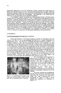
MATERIAL-EXPERIMENTAL PROCESS The starting material was semi-insulating and nearly dislocation-free single crystal doped with 0.3%at.In. Rectangular specimens were cut from 200 gm thick (001) wafers in the dimensions 20 mm along x = (110] and 10 mm along y [110]. Dislocations sources were introduced by a diamond scratch parallel to x at room temperature. Dislocations were generated from these sources by a bending stress at temperatures between Mat. Res. Soc. Symp. Proc. Vol. 262. ©1992 Materials Research Society
592
250 and 500'C, as elongated half loops running along directions in (111) and (111) planes. They got two a (resp. P) 600 segments : one parallel to the free surface, the other emerging at this surface; the third segment was an emerging screw. So half loops could be either a-aX-screw or P-P-screw.It can be demonstrated from geometrical considerations, that depending on the sign of the applied stress, only one type (a-ascrew, or P-P-screw) of half loop can be developed on a given face of the sample. i) In a first series of experiments, we measured the velocities of fresh dislocations. The sample was fixed at the end x = 0 and stressed by cantilever bending (bending axis parallel to y , stress range : 0 - 20 MPa) . In t
Data Loading...