Interface characterization of epitaxial Ag Films on Si(100) and Si(111) grown by molecular beam epitaxy
- PDF / 3,297,615 Bytes
- 10 Pages / 594 x 774 pts Page_size
- 37 Downloads / 323 Views
I.
INTRODUCTION
IN recent years, there has been a growing interest in the microscopic structure of interfaces and films for metalsemiconductor heteroepitaxial systems with a large lattice mismatch (-25 pet), such as A1 or Ag on Si. t~-4] These systems are scientifically and technologically important. From the materials science perspective, it is important to understand the mechanisms by which large area epitaxy can be achieved between systems with such a large lattice mismatch. From the technological point of view, these metal-semiconductor epitaxial systems have a high potential for the application of thermally stable Schottky barrier formation and high-conductivity metallization with a long electron-migration lifetime in very large scale integrated (VLSI) circuit technology.* *Some earlier works in the study of AI/Si interfaces are pertinent to the present investigation. See, for example, F.K. LeGoues, W. Krakow, and P.S. Ho: Phil. Mag. A, 1986, vol. 53, pp. 833-41.
For systems of large lattice mismatch, such as Ag and Si, epitaxial formation may be interpreted as a result of plane matching between Ag and Si. Both Ag(100)/Si(100) and Ag(111)/Si(111) systems have four fdrn lattice planes matched to three Si lattice planes with only 0.33 pet effective difference in mismatch. The initial growth mode and structure of the Ag/Si(111) K.-H. PARK, formerly Graduate Student, Department of Physics, Rensselaer Polytechnic Institute, is Staff Member with the Electronics and Telecommunication Research Institute, Daeduk Science Town, Daejeon, 302-350 Korea. G.A. SMITH, formerly Graduate Student, Department of Physics, State University of New York at Albany, is Associate Staff Member with General Electric Research and Development Center, Schenectady, NY 12301. K. RAJAN, Associate Professor, Department of Materials Engineering, and G.-C. WANG, Associate Professor, Department of Physics, are with the Rensselaer Polytechnic Institute, Troy, NY 12180-3590. This paper is based on a presentation made in the symposium "Interface Science and Engineering" presented during the 1988 World Materials Congress and the TMS Fall Meeting, Chicago, IL, September 26-29, 1988, under the auspices of the ASM-MSD Surfaces and Interfaces Committee and the TMS Electronic Device Materials Committee. METALLURGICAL TRANSACTIONS A
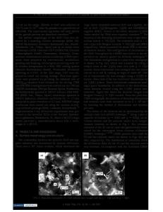
system have been extensively studied using various surface analysis techniques. Previous studies show that Ag grows on the Si(111) surface in the Stranski-Krastanov growth mode with the (V~ x V~) R 30 deg structure. [5'6'7] Recent transmission electron microscopy (TEM) results show that twinned Ag(111) forms on Si(111) with a four to three lattice plane matching, t4j However, few studies are available for the Ag/Si(100) system, and previous results show that either Ag(100) or A g ( l l l ) islands are epitaxially formed on Si(100) substrates, is,91 It is well known that the initial stage of thin film growth is important in determining the epitaxial formation. However, the formation of a thick film which occurs at a later stag
Data Loading...