Interface Structure and Zn Diffusion in the CdTe/ZnTe/Si System Grown by MBE
- PDF / 3,050,197 Bytes
- 6 Pages / 417.6 x 639 pts Page_size
- 19 Downloads / 268 Views
Mat. Res. Soc. Symp. Proc. Vol. 589 @ 2001 Materials Research Society
Oxide removal was achieved by heating to -850'C while monitoring with RHEED until a clean unreconstructed surface appeared. High purity sources of solid CdTe, ZnTe, As, and Te were used for growth. After oxide removal, the wafer was then cooled down under As 4 flux (partial pressure -5x10- 7 torr) to -450 'C, which resulted in a Si(l1 l):As lxl surface. The growth sequences for two particular samples identified as A and B are summarized in the following: Sample A: CdTe/ZnTe/Si (111) A thin ZnTe buffer layer was deposited at -220'C to a thickness of -200A. The ZnTe buffer was then annealed to -31 0°C under Te2 (partial pressure -5x 10⁷ torr) and CdTe fluxes for 10 minutes and a weak surface reconstruction was visible, indicating the smoothness of the single-domain (111 )B surface. The wafer was then exposed to Te2 flux for 5 minutes, and the growth of CdTe was initiated at --3 10°C using a stoichiometric flux. The growth rate was about 1.0 jtm/h.
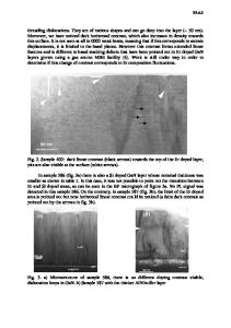
Sample B : CdZnTe/CdTe/ZnTe/Si(21 1) A ZnTe buffer layer was deposited at -220 0 C to a thickness of -70A. It was annealed to -240'C, then 310 'C under Te 2 and ZnTe fluxes for 30 s and 90 s. The CdZnTe layer was deposited on a -2pjim CdTe buffer layer which was grown at 310 'C. Initially, the CdZnTe was graded from x=0 to x-4% over about 1 ptm. Then, CdZnTe was deposited with x-4% to a thickness of -~5m. High-Resolution Electron Microscopy Cross-sectional TEM specimens were prepared by the standard rod and tube method. The specimen preparation procedure involved mechanical polishing to a thickness of about 110-150 gim, followed by dimpling to about 20 to 50 gim, and argon ion-beam milling to perforation using a liquid-nitrogen-cooled sample stage at an angle 150 with a voltage of 5 kV. The samples were finished with 12' and 1.5-2 kV to remove the amorphous surface layer. TEM observations were made with a JEM-4000EX microscope having an interpretable resolution limit of about 1.6A at the operating voltage of 400 kV. Typical observation directions are those which are perpendicular to Si{ 1l0} planes. Images were recorded at close to the optimum objective lens defocus ( - 480A). Both bright-field and dark-field images of the interface region were studied. The contrast of high-resolution bright-field images was enhanced by Fourier filtering to reveal the atomic arrangement at the interface. The analysis of (002) and (004) dark-field images was based on the fact that the structure factors for (002) or (004) reflections are given, respectively, by a difference or sum of the scattering factors of the elements [4]. Enermy Dispersive X-ray Spectroscopy High spatial resolution energy-dispersive x-ray spectroscopy (EDX) was performed with a VG HB501 scanning transmission electron microscope (STEM) operating at 100 kV with a windowless Link EDX detector. This instrument is equipped with a field-emission gun and is capable of forming small electron probes approximately I nm in size. The STEM is interfaced to an EMi
Data Loading...