Investigation of Highly c -axis Oriented AlN Thin Film Re-growth
- PDF / 731,137 Bytes
- 6 Pages / 595 x 842 pts (A4) Page_size
- 65 Downloads / 286 Views
B4.2.1
Investigation of Highly c-axis Oriented AlN Thin Film Re-growth F. Martin1, P. Muralt1 and M. –A. Dubois2 Ceramics Laboratory, Swiss Federal Institute of Technology EPFL, Lausanne, Switzerland. 2 RF microelectronics, CSEM, Neuchâtel, Switzerland. 1
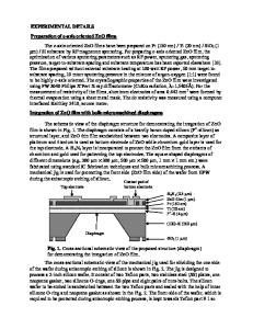
ABSTRACT The properties of AlN films grown on a first set of differently treated AlN films have been studied by XRD, XPS, AFM, in-plane stress and interferometry. All films were deposited by dc pulsed sputtering at 300°C. The first set of films consisted of smooth, pure c-axis oriented AlN monolayers with narrow rocking curve width and excellent piezoelectric coefficient grown on platinized substrate in a large thickness range of 35-2000 nm. Subsequently, a 1000 nm AlN layer has been added. The use of a strongly alkaline developer during intermediate lithography steps and the time elapsed between the two steps of AlN re-growth were found to degrade the overall quality of the films. It’s been shown that the alkaline developer etches down, increases the roughness and contaminates the surface of the AlN monolayer with mainly oxides and hydroxides while the exposure of the films to air develops a native oxide layer. By reducing the air exposure time and by the use of RF plasma cleaning prior to the re-growth process, a good piezoelectric coefficient can be recovered. INTRODUCTION For the past decade, AlN thin films have attracted much attention for high frequency acoustic wave devices, especially thin film bulk acoustic resonator (FBAR) [1]. Although many techniques, such as chemical vapor deposition [2], pulsed laser ablation [3] and molecular beam epitaxy [4] have been used to fabricate AlN thin films on various substrates, the most successful technique for the growth of AlN has been by reactive sputtering [5-7]. Recently, the authors showed that the crystalline improvement during AlN thin film growth by dc pulsed sputtering leads to thickness dependence of functional properties [8]. It would be of great interest to grow multiple thicknesses of AlN on a single wafer as, for example, a system containing both a FBAR filter centered at a carrier frequency and a second similar system set at twice the carrier frequency. This would involve the growth of AlN in two consecutive steps. Such a fabrication requires a screening and a lift-off procedure allowing the AlN re-growth to take place only where required. However, the surface morphology is very sensitive to acid and alkaline chemical agents [9-11]. Hence, it is a major challenge to re-grow AlN thin film whilst retaining most of its structural and functional properties. The parameters of interest are: crystalline tilt, piezoelectric coefficient d33,f, surface contamination, surface roughness and residual mechanical stress. EXPERIMENTAL The 4 inches diameter, 525 µm thick Si (100) substrates were prepared with a 100 Å Ti adhesion layer and a 1000 Å (111)-oriented Pt electrode. AlN thin films were prepared by reactive pulsed direct current (dc) magnetron sputtering in a cluster tool including a transport chamber and load-
Data Loading...