Investigation of phase separation in InGaN alloys by plasmon loss spectroscopy in a TEM
- PDF / 547,342 Bytes
- 8 Pages / 432 x 648 pts Page_size
- 64 Downloads / 349 Views
MRS Advances © 2016 Materials Research Society DOI: 10.1557/adv.2016.542
Investigation of phase separation in InGaN alloys by plasmon loss spectroscopy in a TEM Xiaoyi Wang1, Marie-Pierre Chauvat2, Pierre Ruterana2 and Thomas Walther1* 1 2
Dept. Electronic & Electrical Eng., University of Sheffield, Mappin St., Sheffield S1 3JD, UK CIMAP, UMR 6252, CNRS-ENSICAEN-CEA-UCBN, 14050 Caen, cedex, France
*
Email: [email protected]
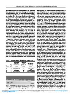
ABSTRACT Phase separation of InxGa1-xN alloys into Ga-rich and In-rich regions was observed by a number of research groups for samples grown with high indium content, x. Due to the radiation sensitivity of InGaN to beam damage by fast electrons, high-resolution imaging in transmission electron microscopy (TEM) or core-loss electron energy-loss spectroscopy (EELS) may lead to erroneous results. Low-loss EELS can yield spectra of the plasmon loss regions at much lower electron fluxes. Unfortunately, due to their delayed edge onset, the low energetic core losses of Ga and In partially overlap with the plasmon peaks, all of which shift with indium content. Here we demonstrate a method to quantify phase separation in InGaN thin films from the low-loss region in EELS by simultaneously fitting both plasmon and core losses over the energy range of 13-30eV. Phase separation is shown to lead to a broadening of the plasmon peak and the overlapping core losses, resulting in an unreliable determination of the indium concentration from analyzing the plasmon peak position alone if phase separation is present. For x=0.3 and x=0.59, the relative contributions of the binary compounds are negligibly small and indicate random alloys. For xnom.=0.62 we observed strong broadening, indicating phase separation. INTRODUCTION Optoelectronic devices based on ternary InGaN alloys can cover a wide range of optical emission and absorption, from near ultraviolet (GaN) to infrared telecom wavelengths (InN). However, InGaN growth is a complex process and a number of phenomena such as ordering [1] crystallographic defects [2] as well as phase separation [3] may significantly influence the device performance [4-6]. Phase separation of InxGa1-xN alloys into Ga-rich and In-rich regions was first predicted by Ho and Stringfellow [7] and later observed by a number of research groups. InGaN samples grown at high temperatures are particularly prone to this. As the indium concentration controls the optical emission properties of InGaN it is important to quantify any degree of phase separation in an InGaN thin film. However, due to the radiation sensitivity of InGaN to beam damage by fast electrons, as observed by O’Neill et al. [8] and Smeeton et al. [9], high electron fluxes as typically used in extended high-resolution imaging in transmission electron microscopy (TEM) or core-loss electron energy-loss spectroscopy (EELS) may lead to erroneous results. Low-loss EELS can yield spectra of the plasmon loss regions at much lower electron fluxes and so potentially prevent or at least reduce beam damage in the TEM. Unfortunately
Data Loading...