Investigation of the Optical Properties of epitaxial-lateral-overgrown GaN on R- and M- plane Sapphire
- PDF / 2,065,179 Bytes
- 4 Pages / 612 x 792 pts (letter) Page_size
- 89 Downloads / 324 Views
0955-I12-04
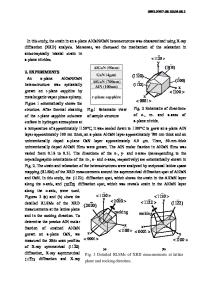
Investigation of the Optical Properties of epitaxial-lateral-overgrown GaN on R- and Mplane Sapphire Tobias Guhne1, Zahia Bougrioua1, Martin Albrecht2, Phillippe VennÈguËs1, Mathieu Leroux1, Marguerite La¸gt1, Sosse Ndiaye1, Monique Teisseire1, Luan Nguyen1, and Pierre Gibart1 1 CRHEA-CNRS, Rue Bernard GrÈgory, Valbonne, 06560, France 2 Institut f¸r Kristallz¸chtung, Max-Born-Strasse 2, Berlin, 12489, Germany INTRODUCTION Todayís C-plane quantum-well based GaN optoelectronics suffer from a reduced efficiency and a red-shift of the optical transitions as a result of the polarization induced Quantum Confined Stark Effect (QCSE). Non- or semipolar GaN based emitters would therefore show improved optical properties, because in such crystal orientation polarization induced interfacial charges are annihilated or drastically reduced. By growth on R-plane-sapphire, GaN is oriented along the nonpolar [11-20] direction, whereas growth on M-plane-sapphire delivers a so called semipolar orientation, along the [1013] or [11-22] directions, depending on the nitridation temperature. First demonstrations of UV, blue and green light emitting diodes realized on nonpolar and semipolar GaN were published recently. Nevertheless the lack of adapted substrates does not yet allow the growth of reduced polarity GaN with decent crystal structure. Mainly large densities of basal stacking faults (BSF), in the range of ~105-107 cm-1, are present. Epitaxial-lateral-overgrowth (ELO) is known as an efficient way of filtering defects in polar GaN. Craven et. al showed, that it can be used as well on nonpolar GaN [1]. In this work we investigate nonpolar and semipolar fully coalesced GaN ELO-templates in order to identify the existing defects and to localize them in the samples. Therefore low temperature cathodoluminescence (CL) was used to investigate the spatial distribution of the defects in conjunction with transmission electron microscopy (TEM) to study the microstructure. EXPERIMENTAL DETAILS All samples were grown in a vertical Metal-Organic-Vapor-Phase-Epitaxy reactor under typical conditions for out of C-axis GaN growth already published elsewhere [2]. On a highly defective GaN template, grown on R- or M-plane sapphire, a mask of SiN was evaporated. Stripes were then processed, such as they are situated perpendicular to the GaN C-axis of width of 3/7 µm leaving an open window of 2/3 µm between the stripes on semipolar or nonpolar GaN templates. Regrowth was undertaken on the so prepared templates in order to obtain GaN material of reduced defect density in the mask overgrown region. Cross-section slices of GaN samples were prepared for TEM and CL study. RESULTS TEM images of non- and semipolar ELO-GaN are shown in cross section view in Fig.1a and b. Two regions can be identified in both samples: the defective seed, the region above the window, and the overgrown wing region. TEM investigations revealed, in the nonpolar GaN seed layer, a high density of different defects: basal stacking faults (BSF) with an average
density of 4