Ion Irradiation Induced Grain Growth in Metal Thin Films
- PDF / 1,947,185 Bytes
- 6 Pages / 420.48 x 639 pts Page_size
- 113 Downloads / 419 Views
ION IRRADIATION INDUCED GRAIN GROWTH IN METAL THIN FILMS JOYCE.C. LIU AND J.W. MAYER Department of Materials Science University, Ithaca, NY 14853
and
Engineering,
Cornell
ABSTRACT The dependence of ion irradiation induced grain growth on collision and material properties were studied in metal and alloy thin films. The uniform grain size increased with ion dose in the low dose regime; and the growth saturated in the high dose regime. The saturated grain size was determined 'by the cascade dimension as well as the atomic mobility. The growth was further influenced by the temperature, composition and impurity. INTRODUCTION Ion irradiation induced grain growth has been studied in pure metal, alloy and semiconductor materials[i-5]. Van Wyk[l] investigated the preferential growth of oriented Cu grains after irradiation. A pronounced grain growth was found in the mixed Aus0Niso metastable phase(21. The grains grew linearly with ion dose in Ag÷ implanted Ni films[3]. A weak temperature dependence of grain growth at 400-500°C was observed in self-implanted Ge films[4]. A homogeneous grain growth was found in irradiated Ni films in comparison to the non-uniform growth induced by thermal annealing at 2000C[5]. In this paper, we will present some experimental results of ion irradiation induced grain growth in metal thin films. The objective is to study the dependence of radiation induced grain growth on properties of the collision cascade by use of different ion species and of the atomic mobility by use of alloys, different substrate temperatures and introduction of impurities. SAMPLE PREPARATION
of
Pure metal thin films of Ni,
Ni Cu30
and
Ni 30Cu7
were
evaporavion and co-evaporation
at
Cu, Pd and Pt and alloy
prepared room
by
electron
temperature
and
films
beam
base
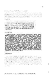
pressure less than 3x10torr. The thickness of the films ranged from 50-70 nm. In order to prevent preferential orientation of the grains, the films were deposited on SiO substrates coated with positve photoresist and then floated ofi in acetone. The separated films were rinsed in deionized water before mounting on transmission electron microscopy(TEM) grids for subsequent irradiations and TEM observations. RESULTS AND DISCUSSION Collision Effect In the as-deposited polycrystalline Ni thin films, the randomly oriented grains have an average diameter of 9 nm. Irradiation with 240keV Ar÷ , 310keV Kr"÷ and 560keV Xe++ ions, where the projected ranges were equivalent to or larger than the film thickness, induced a homogeneous grain growth in the Ni films. An increase in grain size from 9 to 40 nm with the
M&LRe&. Smc. Syrup. Proc. Vol. 100. ©19i Materiels Research Socily
358
M•
As deposited
B4X1014 Xe/cm
b
B9x10
c 2xlO'5 Xe/cm
2
15
2
Xe/cm
4
Fig. 1. Dark field images and electron diffraction patterns of Ni films showing the enlargement of grain size with dose after 560keV Xe ion irradiation at room temperature. increase of ion dose after Xe*÷ irradiation is observed from TEM micrographs shown in Fig. 1. The development of spotty rin
Data Loading...