Large Grain Size and High Deposition Rate for Microcrystalline Silicon Prepared by VHF-GD
- PDF / 1,076,902 Bytes
- 6 Pages / 414.72 x 648 pts Page_size
- 27 Downloads / 345 Views
ABSTRACT
The growth mechanism and material properties of -type pic-Si:H prepared with plasma enhanced chemical vapour deposition in the very high frequency range is investigated. By increasing the plasma excitation frequency the grain size, deposition rate and Hall mobility can be simultaneously increased without having to adjust other deposition parameters in particular the temperature. This effect is explained by an enhanced selective etching of amorphous tissue and grain boundary regions together with a sufficient supply of growth species at high frequency plasmas.
INTRODUCTION
Microcrystalline silicon ([ic-Si:H) is commonly prepared by plasma enhanced chemical vapour deposition (PECVD) from gas mixtures of SiH4 and H2 at temperatures as low as 30 0 C [1,2]. The deposition process is compatible with the well established amorphous silicon (a-Si:H) technology which makes Rc-Si:H a promising material for applications in large area electronic devices like thin film solar cells and flat panel displays [31. In addition the material has potential as nucleation seed for thin crystalline silicon. For technical applications a further improvement of the carrier mobility, the grain size and the deposition rate is required. In particular, generally a correlation between crystallinity and suppressed growth rate is found [4] and an improvement of the grain size is mainly achieved by an increase in the deposition temperature [5]. High temperatures, however, one wants to avoid in amorphous silicon technology and large area electronics. Recently the use of very high frequency glow discharge (VHF-GD) was proposed to provide favourable conditions for the growth of pc-Si:H, leading to high quality material at lower plasma excitation power and deposition temperatures [ 1,2,6]. The influence of the plasma excitation frequency (uex) on the process plasma and the film nucleation is still not well understood. Likely effects are a reduction of the plasma sheath potentials, sheath thickness and a higher dissociation of the process gases [7-10]. While detailed studies of the processes in the plasma and the film growth zone are rather complicated, we concentrate on the influence on the end product: the microcrystalline or amorphous Si film. Here we present an investigation on material prepared with PECVD in the frequency range 13 - 120 MHz.
745 Mat. Res. Soc. Symp. Proc. Vol. 358 @1995 Materials Research Society
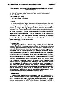
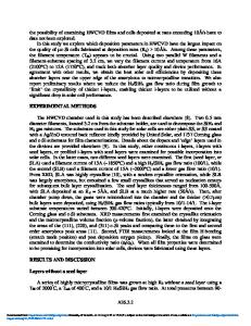
1.6 y-v,
H*-.
500 mTorr 300 mTorr 150 mTorr
1.2 L
plasma power. 50 rrW/cm 2
plasma por. 50 nAAcn? 60-
(D
0.8
+ 40-
UPS
"0.4 20 ........... 0 1. . . . . . . . . . . ..
0,
0
25
50
75
100
0
125
25
50
75
100
125
Plasma exdtation frequency v [Mv-Hz]
Plasma excitation frequency v [MHz]
Fig. 2 Intensity ratio of the integrated Raman intensities of the crystalline (Ic at 520 cm" 1) and the amorphous (Ia at 480 cm- 1) signal strength.
Fig. 1 Deposition rate as a function of the plasma excitation frequency. The deposition rate increases with frequency and pressure. EXPERIMENT
Samples were prepared in a standar
Data Loading...