Low Pressure Organic Vapor Phase Deposition of Small Molecular Weight Organic Device Structures
- PDF / 2,211,603 Bytes
- 6 Pages / 414.72 x 648 pts Page_size
- 44 Downloads / 329 Views
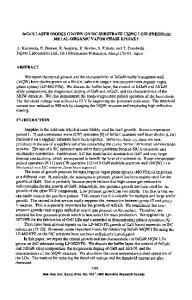
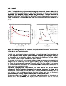
ABSTRACT A new technique for the deposition of amorphous organic thin films, low pressure organic vapor phase deposition (LP-OVPD), was used to fabricate organic light emitting devices (OLEDs) and optically pumped organic lasers. The OLED consisted of a film of aluminum tris(8 hydroxyquinoline) (Alq 3) grown on the surface of a film of N'-diphenyl-N,N'-bis(3methylphenyl)1-l'biphenyl-4-4'diamine (TPD). Growth on both glass and polyester substrates was accomplished and the resulting heterojunction devices were found to have a performance similar to conventional, small molecular weight OLEDs grown using thermal evaporation in vacuum. The LP-OVPD grown OLED has an external quantum efficiency of 0.40 ± 0.05% and a turn-on voltage of approximately 6V. The optically pumped organic laser consisted of a film of Alq 3 doped with the laser dye, benzoic acid, 2-[6-(ethylamino)-3-(ethylimino)-2,7-dimethyl-3Hxanthen-9-yl]-ethyl ester, monohydrochloride (Rhodamine 6G). The laser output was centered at approximately 610nm and the lasing threshold was 3OpLJcm 2 . The rapid throughput of LP-OVPD and its use of low vacuum in a horizontal reactor demonstrate its potential to facilitate low cost, roll-to-roll deposition of organic films for many photonic device applications. INTRODUCTION The field of organic electroluminescence is attracting rapidly growing commercial interest, spurred by possible applications in lucrative markets such as video displays. Both small molecule and polymer-based organic devices have been investigated, but polymer-based devices have the advantage of simple and perhaps inexpensive fabrication by spin-on deposition techniques. In contrast, small molecular weight devices are usually fabricated by thermal evaporation in vacuum. This is often considered to be a more expensive process. However, a new organic film growth technique, organic vapor phase deposition (OVPD) [1,2,3] may eliminate this apparent disadvantage, leading to very low cost, large scale deposition of small molecular weight organic layers for numerous photonic device applications. Similar to the process of vapor phase epitaxy commonly used in the growth of Ill-V semiconductors, OVPD uses carrier gases to transport vapor from the source to the substrate where it condenses to form the desired thin film. However, films grown using this technique at atmospheric pressure are often found to have non-uniform surface morphologies due to gas phase nucleation and a diffusion-limited growth process [2]. These effects were also observed by us when atmospheric pressure OVPD was used to deposit small molecular weight organic materials for use in OLEDs. Following the example of the growth of III-V films by organometallic vapor phase epitaxy, more uniform organic film growth should be possible at reduced pressures. This is 587 Mat. Res. Soc. Symp. Proc. Vol. 488 ©1998 Materials Research Society
due in part to lower concentrations of organic materials in the deposition chamber, minimizing gas phase nucleation. Also, low pressures can result in kinetically-contr
Data Loading...