Low Temperature Formation of Silicon Nitride Film: Combination of Catalytic-Nitridation and Catalytic-CVD
- PDF / 177,899 Bytes
- 6 Pages / 595 x 842 pts (A4) Page_size
- 30 Downloads / 299 Views
LOW TEMPERATURE FORMATION OF SILICON NITRIDE FILM : COMBINATION OF CATALYTIC-NITRIDATION AND CATALYTIC-CVD A. Izumi, A. Kikkawa and H. Matsumura JAIST (Japan Advanced Institute of Science and Technology) Ishikawa 923-1292, JAPAN, [email protected] ABSTRACT In this work silicon nitride films are formed as substrate temperatures 250oC by combination of catalytic-nitridation and catalytic-vapor deposition method in a catalytic chemical vapor deposition system. It is found that inserting nitridation layer about 2 nm-thick before growing the silicon nitride films, injection-type hysteresis of capacitance-voltage curve is drastically reduced from 1.4 V to 0.05 V for 40 nm-thick SiNx. INTRODUCTION The future flat-panel displays (FPD) having larger diagonal-size, more pixel and better gradient, high-performance thin-film transistors (TFTs) are receiving much attention for use in high quality liquid-crystal displays (LCD). It is essential to improve the electrical characteristics of the Si films as the active layer and of the gate dielectrics, such as SiO2 and silicon nitride (SiNx). SiNx films prepared at low temperatures below 400oC are widely applicable as gate dielectric films used in LCD TFTs. Plasma-enhanced CVD (PECVD) method is one low temperature methods of deposition. However, PECVD has serious problems, such as plasma damage to the substrates. M oreover, large area deposition of SiNx films by the conventional radio frequency PECVD becomes difficult because the standing waves in radio frequency plasmas limit uniform power dissipation. Therefore, a novel method to obtain SiNx films in large area at low temperatures, without any help from plasma excitation, is strongly required. The catalytic chemical vapor deposition (catalytic-CVD) method [1], which is often called hot-wire CVD (HWCVD), is one method to answer above requirement. In this method, deposition gases are decomposed by the catalytic cracking reactions of a heated tungsten (W) catalyzer placed near substrates. SiNx films are formed at low temperature, as low as around 300oC, without any help from a plasma or photochemical excitation [2,3]. Recently, we have succeeded in depositing amorphous-Si on a large glass substrate (1000 x 400 mm) with uniformity of 7.5 % [4]. Low-temperature direct nitridation of crystalline Si below 300oC, named catalytic-nitridation can be performed using decomposed NH3 species in a catalytic-CVD system [5]. It is well known that the quality of interface between gate dielectric films and semiconductors determines the electrical properties of TFTs. Inserting a nitridation layer before SiNx deposition may improve the quality of interface.
A10.3.1 Downloaded from https://www.cambridge.org/core. Access paid by the UCSB Libraries, on 24 Jul 2018 at 15:33:56, subject to the Cambridge Core terms of use, available at https://www.cambridge.org/core/terms. https://doi.org/10.1557/PROC-715-A10.3
In this work, electrical properties of SiNx films formed around 250oC by combination of direct nitridation and SiNx deposition in a catalytic-CV
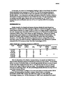
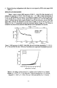
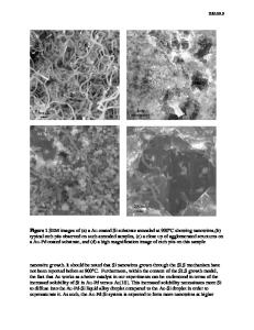
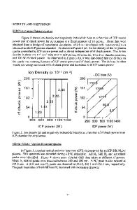
Data Loading...