Macroscopic Actuators Using Thick Piezoelectric Coatings
- PDF / 3,682,834 Bytes
- 11 Pages / 612 x 792 pts (letter) Page_size
- 19 Downloads / 400 Views
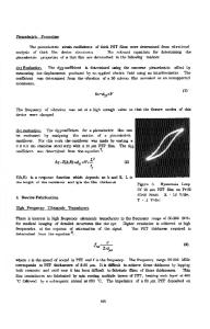
Macroscopic Actuators Using Thick Piezoelectric Coatings M. Sayer1, G.R. Lockwood1, T.R. Olding1, G. Pang1, Lester M. Cohen2, W.Ren3 and B.K.Mukherjee3 1 Department of Physics, Queen’s University, Kingston, ON, K7L 3N6, Canada 2 Smithsonian Astrophysical Observatory, 60 Garden St. Cambridge, Mass. 02138, USA 3 Department of Physics, Royal Military College of Canada, Kingston, ON, K7K 7B4, Canada ABSTRACT Large scale actuated structures often require piezoelectric elements in the thickness range 10-50µm. For manufacturing purposes, the chemical solution deposition of sol gel composites can create such structures using methods compatible with semiconductor fabrication technology. The piezoelectric characteristics of structures fabricated by patterning methods based on the lapping and dicing of bulk ceramic, spray coating and laser machined and micromolded sol gel composites are compared. Laser interferometer measurements on PZT/PZT composites give d33 = 200 pC/N and d31 = 24 pC/N. The design and fabrication of large area voltage actuated mirrors and annular and linear ultrasonic arrays in the frequency range of 50 MHz are demonstrated. INTRODUCTION MEMS (micro-electro-mechanical systems) technology incorporates electromechanical actuation into structures micromachined into silicon having dimensions on the scale of 1-20µm [1]. The piezoelectric or electrostrictive actuating element has a thickness compatible with this scale, e.g. 0.5-3µm. Such elements may be created by chemical solution deposition (sol gel or metallorganic decomposition), physical sputtering or pulsed laser deposition. An important class of larger actuated structures exist in which either the desired properties result from the dimensions of the structure, or in which forces need to be applied to structures having large size or complex geometry [2]. These macroscopic applications generally require a film thickness in the range 20 to 200µm and include mechanical resonators, large area structures on metal and glass, complex surfaces such as optical fiber and systems which require multielement actuation. In these applications, actuation has generally been accomplished using strategically placed bulk discrete ceramic elements [3]. Examples of such structures are ultrasonic and surface acoustic wave transducers and arrays, unimorph and bimorph actuators, ink jet printer heads and active damping systems. Common problems in the implementation of such devices are the cost and complexity of assembly, the method of interconnection and the incorporation of external circuitry, and limited opportunities for batch fabrication. In this paper we discuss the application of sol gel composites to this problem, use interferometer methods to show comparative performance characteristics with respect to bulk ceramics, and illustrate device design by specific examples. MATERIAL FABRICATION AND CHARACTERIZATION Sol gel composite coatings are prepared by depositing a suspension of a powder in a sol gel solution on a substrate and firing [4,5]. Fabrication of large area coatings
Data Loading...