Manipulation and Control of Nucleation and Growth Kinetics with Hydrogen Dilution in Hot-Wire CVD Growth of Poly-Si
- PDF / 317,513 Bytes
- 5 Pages / 612 x 792 pts (letter) Page_size
- 28 Downloads / 315 Views
Manipulation and Control of Nucleation and Growth Kinetics with Hydrogen Dilution in Hot-Wire CVD Growth of Poly-Si Maribeth Swiatek, Jason K. Holt, David G. Goodwin, and Harry A. Atwater Thomas J. Watson Laboratory of Applied Physics California Institute of Technology, Pasadena, CA, 91125. ABSTRACT We systematically explore the relationship between gas-phase kinetics and film microstructure in the hot-wire CVD technique using diluted silane (1% in He) and additional hydrogen. Using a wire temperature of 2000ºC, films were grown on Si (100) at 300ºC using 1 mTorr SiH4 and 99 mTorr He at hydrogen pressures from 0-100 mTorr. Transmission electron microscopy and atomic force microscopy measurements indicated that continuous microcrystalline films had a columnar grain structure and that grain size increased from 40 nm using SiH4/He to 85 nm using SiH4/He/H2 with 20:1 H2:SiH4 ratio due to the etching of silicon by hydrogen. Etching rate measurements using a quartz deposition monitor show that, under the current deposition conditions, a transition from net film growth (0.17 nm/s using only SiH4) to net etching occurs at a H2:SiH4 ration of 80:1. The effect of atomic H on the nucleation density during the initial stages of growth has also been investigated, revealing a sublinear dependence of nucleation density with time and a decrease in nucleation density with increasing H2 dilution. High deposition rate growth with no H2 dilution has been achieved on a low-density array of seed nuclei produced using high H2 dilution. INTRODUCTION Hot wire chemical vapor deposition (HWCVD) is an attractive method for growth of polycrystalline silicon thin films for application in thin film polycrystalline silicon photovoltaics [1,2]. A key issue is to identify growth conditions that enable the largest possible grain size at a given growth temperature with low intragranular defect density. Hydrogen is known to play a critical role in the development of a crystalline microstructure in both polycrystalline [3, 4] and epitaxial [5] films grown by HWCVD at low temperatures. The role of atomic hydrogen produced by the wire in the etching of amorphous Si and small crystalline nuclei and its effect on the resulting film microstructure are investigated. EXPERIMENT All HWCVD experiments were performed at pressures of no higher than 1x10⁻⁵ Torr. A 0.25 mm diameter W wire was resistively heated to 2000ºC and positioned at a distance of 2.5 cm from the substrate. The wire was used to radiatively heat substrates of
A19.2.1
100 nm SiO2 on Si to 300ºC. H2 dilutions are referenced to 1 mTorr of SiH4 in 99 mTorr He; all gases used are ultrahigh purity. A translatable shutter between the wire and substrate was used to enable several growth experiments at identical gas ambient and wire temperature on each substrate at low Si coverage, as well as to provide a definite starting and ending point for film growth. RESULTS
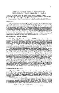
0.08
0.008
0.06
0.007 0.006
0.04
0.005 0.02 0.004
Net rate (nm/sec)
0.00
Silane mole fraction
0.003
-0.02
0.002
-0.04
0.001
Data Loading...