Material properties and growth process of microcrystalline silicon with growth rates in excess of 1 nm/s
- PDF / 57,039 Bytes
- 6 Pages / 595 x 842 pts (A4) Page_size
- 2 Downloads / 365 Views
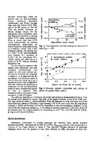
Material properties and growth process of microcrystalline silicon with growth rates in excess of 1 nm/s E.A.G. Hamers1, A.H.M. Smets1, C. Smit2, J.P.M. Hoefnagels1, W.M.M. Kessels1, and M.C.M. van de Sanden1 1 Eindhoven University of Technology, P.O. Box 513, 5600 MB Eindhoven, the Netherlands 2 Delft University of Technology, DIMES, P.O. Box 5053, 2600 GB Delft, the Netherlands ABSTRACT The expanding thermal plasma (ETP) has been used to deposit microcrystalline silicon (µc-Si:H) with rates up to 2.7 nm/s. Typical material properties of well crystallised material are crystallite sizes of 20 nm, photo- and dark conductivity of 2x10⁻⁵ and 2x10⁻⁷ S/cm respectively, and an activation energy of 600 meV. The radical densities of SiH3, SiH, and Si present in the gas phase have been quantified. In conditions where µc-Si:H is deposited the atomic hydrogen flux towards the surface is of the same magnitude or higher as the flux of deposited radicals. Furthermore, the abundance of radicals such as SiH and Si is large and may contribute several tens of percent to the deposition rate. INTRODUCTION The deposition of µc-Si:H is often achieved by diluting silane in hydrogen. Issues in the research on this material include the growth mechanism, and especially the role of atomic hydrogen in it, and obtaining high growth rates [1,2,3]. Since microcrystalline silicon has a lower absorption coefficient than a-Si:H in the visible part of the spectrum, the layers have to be thicker (several microns) when implemented in a solar cell. Higher growth rates than that currently achieved are therefore required. Two techniques to deposit µc-Si:H are radio frequent plasma enhanced chemical vapour deposition (RF-PECVD) and hot wire or catalytic chemical vapour deposition (HW- or CatCVD). In RF-PECVD electrons gain energy in an oscillating electric field and dissociate the silane and hydrogen by electron impact. Under conditions for µc-Si:H deposition ions are an abundant species [4]. In HW-CVD the radicals are created by dissociation of silane and hydrogen at a hot, typically 2000 K, tungsten filament. The radicals may react in the gas phase or at the surface leading to the growth of a silicon containing film. Since several years we deposit a-Si:H with an expanding thermal plasma and study its growth process. The thermal plasma is created at pressures of 0.5 bar in a mixture of argon and hydrogen and under these conditions the plasma is a source of atomic hydrogen. This plasma expands into a low-pressure (20 Pa) vessel in which silane is injected. The atomic hydrogen reacts with the silane and creates silane radicals by hydrogen abstraction. The expanding plasma transports the radicals to the substrate 35 cm further downstream. Under a-Si:H deposition conditions SiH3 is the most important radical while growth rates of 7 nm/s are obtained [5]. In this paper we will demonstrate that we can deposit µc-Si:H silicon at rates up to 2.7 nm/s using the expanding thermal plasma. Different radicals present during the deposition are measured and their densit
Data Loading...