Measuring the Strength and Stiffness of Thin Film Materials by Mechanically Deflecting Cantilever Microbeams
- PDF / 2,179,000 Bytes
- 6 Pages / 420.48 x 639 pts Page_size
- 99 Downloads / 238 Views
MEASURING THE STRENGTH AND STIFFNESS OF THIN FILM MATERIALS BY MECHANICALLY DEFLECTING CANTILEVER MICROBEAMS T. P. WEIHS, S. HONG, J. C. BRAVMAN and W. D. NIX Department of Materials Science and Engineering Stanford University, Stanford, CA, 94305. Abstrac
The present authors recently introduced the mechanical deflection of cantilever microbeams as an experimental technique for measuring the strength and stiffness of thin films.[1] The technique utilizes conventional integrated circuit (IC) fabrication to process the samples, a Nanoindenter to deflect the cantilever beams mechanically, and simple elastic beam theory to analyze the data. This paper will review the technique and describe some of its current applications.
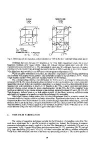
Introduction When measuring the mechanical properties of thin films, the presence of substrates below the films can affect the measurements[2]. Thus, one would prefer to test the films free of their substrates. However, if the films are approximately 1.0 Ptm thick and free-standing, they can be damaged if handled directly. To avoid both of these problems, and to offer a measurement of the strength and stiffness of thin films on a local scale, the deflection of cantilever microbeams using a Nanoindenter was introduced recently[l]. This paper will describe the three basic stages of the microbeam technique - the fabrication of samples, the testing of samples, and the analysis of data. In addition, some applications of the technique will be described and several issues regarding the deformation of the beams will be discussed. Sample Fabrication A variety of different materials can be fabricated into cantilever beams for testing.
Interconnect metals such as gold, dielectric materials like silicon dioxide, and semiconductors such as silicon have all been tested- For such a diverse group of materials, different IC processing methods are employed. The first method -- called the "lift-off" technique -- is typically used in the processing of metal beams. It is termed "lift-off' because photoresist is peeled away or "lifted off" the silicon substrate in order to pattern the metal film. The initial step in the technique is the deposition and patterning of photoresist. A positive resist is spun onto a lightly-doped p-type (100) silicon wafer and patterned using typical exposures to UV light and chemicals. The processing leaves photoresist only in sections where the metal film is not desired. In the next step, metal is deposited over the complete top side of the wafer using e-beam evaporation or sputtering techniques. After the deposition, warm acetone dissolves the photoresist that is covered by the metal film and thereby lifts off the unwanted sections of the film The cantilever beams then appear as thin lines on the silicon. To form the bottom side of the cantilever beams, a heated solution of EDP (66 wt.% ethylendiamine, 23 wt.% H2 0, 11 wt.% pyrocatechol) anisotropically etches away the silicon from below the metal lines. The final sample will appear as shown in Figure 1: cantilever beams extending over an
Data Loading...