Mechanical Behavior of Contact Aluminum Alloy
- PDF / 1,769,114 Bytes
- 6 Pages / 612 x 792 pts (letter) Page_size
- 93 Downloads / 435 Views
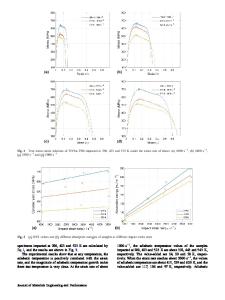
Mechanical Behavior of Contact Aluminum Alloy* David T. Read, Yi-Wen Cheng, J. David McColskey, and Robert R. Keller National Institute of Standards and Technology, Materials Reliability Division 325 Broadway, Boulder, CO 80305-3328, USA. ABSTRACT We report the results of tensile tests of thin films of Al-0.5 % Cu deposited on bare silicon. This material was subjected to the complete CMOS fabrication process, including a high-temperature heat treatment. Contact metal makes the electrical connection between the metal wiring and the silicon transistors in a chip. Room-temperature values of yield strength, ultimate tensile strength, and elongation were all lower than the corresponding values found previously for pure electronbeam-evaporated aluminum films. The strengths and elongation decreased slightly as the specimen temperature was raised from 25 to 150 ºC. The slopes of the stress-strain curves from unloading-reloading runs were lower than the accepted Young's modulus of bulk polycrystalline aluminum. The results are interpreted with the help of scanning and transmission electron microscopy. INTRODUCTION Thin films of aluminum have been used for decades to provide electrical connections within integrated circuits. Electrical contact is made to transistors by depositing aluminum on bare silicon adjacent to the gate structure. Transistors are connected to each other by aluminum deposited on the field oxide or the interlayer dielectric. Here we report the results of tensile tests of Al-0.5 % Cu deposited on bare silicon. This material was on a wafer that was subjected to the complete CMOS fabrication process, which includes a high-temperature heat treatment. The exact temperature for this process was not provided by the manufacturer; a typical temperature for this process would be 450 to 500 ºC [1]. Many reports on the mechanical properties of aluminum films can be found in the literature, for example, [2]. However, few of these describe material that had been subjected to the complete fabrication process for microelectronic chips, and we are aware of none that report the tensile properties of 10 µm wide lines of such material, as we do here. Quantitative information about the mechanical properties of this material would be useful in modeling the mechanical reliability of the interconnect structure on a chip MATERIAL AND SPECIMENS Our specimens were thin metal films on "tiny chips" 2 mm square produced by a commercial fabricator under the MOSIS arrangement. We received five chips from a single fab run. Typically such chips would come from different wafers in the run. The fabrication process used to make our specimens includes two metal layers, both Al-0.5 % Cu. The process also includes dielectric and other layers. We used the photolithographic design of our specimens to exclude these layers. -----------------------------------*Contribution of the U. S. government, not subject to copyright in the U. S. A. L6.11.1
We tested two types of specimens: metal 2 (M2) layer only, and both the metal 1 (M1) layer and the metal
Data Loading...