Mechanical Behavior of Nanocrystalline Cu Alloy Thin Film on Elastomer Substrates Under Constant Uniaxial Tensile Strain
- PDF / 552,378 Bytes
- 6 Pages / 612 x 792 pts (letter) Page_size
- 107 Downloads / 384 Views
0976-EE10-09
Mechanical Behavior of Nanocrystalline Cu Alloy Thin Film on Elastomer Substrates Under Constant Uniaxial Tensile Strain Junya INOUE, Yousuke FUJII, and Toshihiko KOSEKI Department of Materials Engineering, The University of Tokyo, 7-3-1 Hongo, Bunkyo, Tokyo, 113-8656, Japan
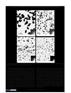
ABSTRACT In this study, mechanical behavior of nanocrystalline Cu alloy thin films under constant tensile strain is studied, by taking advantage of the enhanced resistance to strain localization of a thin metal film on a thick elastomer with appropriate Young’s modulus. Cu and Cu alloy thin films with a thickness of 100nm were deposited on heat-resistant polyimide substrates. On the top of the Cu alloy layer, Ta thin film was further deposited to suppress the surface diffusion of Cu alloy. A uniform uniaxial tensile strain was induced to the films by applying a constant radius of curvature to the polyimide substrate. Isothermal deformation and rupture modes of the films were studied by keeping the samples at various elevated temperatures. Microstructural observation was carried out using SEM, TEM, STEM, and confocal violet laser microscope at several stages of deformation. From the observation, the evolution of damage in the sub-critical strain level and the effect of alloying elements are discussed. INTRODUCTION Cu and Cu alloys are used as interconnection material in microelectronic integrated circuits. In present generation of CMOS devices, interconnection lines are composed of nanocrystalline Cu alloys, because the continuous reduction in device dimensions forces the width of interconnection lines to be in the order of 100 nm. Consequently, the mechanical properties of these nanocrystalline Cu and its alloys can be decisive for their reliability. Among other mechanical behavior of interconnection material, stress induced voiding (SIV) has been one of the most serious reliability concerns since the era of Al interconnects, and has been discussed in the analogy to cavitations during high temperature creep. Hence, most of the study concerning SIV of Cu interconnection line is still discussed from the view point of the void growth rate, which can be associated with stress gradient imposed in interconnection lines[1,2]. However, recent study has revealed that nucleation of void is rather critical in the case of Cu interconnection line than growth of voids, because of its nature of fabricated structure[3]. In the field of mechanics of nanocrystalline metal and alloy, although void formation is also considered to be a dominant mechanism controlling fracture behavior in tension, the evolution of such damage and consequences to final fracture is only beginning to be understood[4]. Few systematic experiments have been conducted to clarify the process, and only a couple of models are proposed based on the observation of dimpled rupture and the results from large scale molecular dynamics simulations[5,6]. The proposed mechanisms responsible for
void initiation are 1) existing voids at grain boundary and triple points, 2) voids created b
Data Loading...