Micro-Indentation and Micro-Scratch Tests on Sub-Micron Carbon Films
- PDF / 1,469,277 Bytes
- 6 Pages / 420.48 x 639 pts Page_size
- 27 Downloads / 397 Views
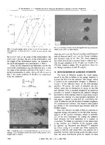
MICRO-INDENTATION AND MICRO-SCRATCH TESTS ON SUB-MICRON CARBON FILMS. T.W. WU*, R.A. BURN*, M.M. CHEN** AND P.S. ALEXOPOULOS* *IBM Research Division, Almnaden Research Center, San Jose, CA 95120. **IBM General Product Division, San Jose, CA 95139. ABSTRACT Micro-indentation and micro-scratch techniques were used to characterize the hardness and the adhesion strength of 0.11 /am thick sputtered carbon f-ilms on Silicon substrates. Hardness depth profiles and critical loads were measured using a microindenter under indentation and scratch testing modes, respectively. The carbon film with 6 mtorr argon sputtering pressure shows better practical adhesion (or higher critical load) and slightly higher hardness. The indentation fracture phenomenon observed on the 30 mtorr f'ilm is closely related to its poor adhesion. The failure mechanism will also be discussed. INTRODUCTION Adhesion is not just an important problem but also a difficult one. Nowadays, extremely thin films ( < 0.1 /pm) are extensively used both in semiconductor and computer storage technologies; therefore, a device which is capable of measuring this critical property of a sub-micron thick f'ilm is highly desirable. The characterization of adhesion strength by scratch testing is well established and commonly used in the hard coatings industry [1-4]. However, because of approximately two orders of magnitude difference in the sample thickness, new specifications are required on the potential testing devices, such as the range and the resolution of the applied load, the sensitivity of the acoustic emission detector, the tip radius and quality of the indenter...etc., and these stringent demands mean conventional type scratch testers are not immediately applicable. In this study, we have modified the existing microindenter developed at the IBM Almaden Research Center [5] to perform not only the micro-indentation but also the micro-scratch tests. Two sub-micron carbon films with different mechanical properties have been used to demonstrate this added capability. Extensive SEM studies were also carried out to understand the failure mechanisms. EXPERIMENTAL PROCEDURE Two 0.11 /pm thick carbon films were deposited on Si < 111> wafers using a DC planar magnetron sputtering system under the same process conditions except for different argon sputtering pressures. The nomenclature, process conditions and some of the sample properties are summarized in Table I. After deposition, the Si wafer was cut into approximately 10 mm square coupons which were mounted on the sample post (2 in Fig.lI) for the indentation and scratch tests. For obtaining the hardness depth profiles, we have performed the continuous load and unload test and utilized the data processing routine described in the previous report [5]. The indentation rate used for the loading and unloading stages were 4 and 15 nm/sec, respectively. The indenter used for hardness measurement was a 3-sided diamond pyramidal or Berkovich indenter
[6].
TABLE I: Some Properties of the Sample Films Sample ID
Ar-pressure (mt
Data Loading...