Microanalysis of Self-assembled InAs Quantum Dot Structures Grown for Infrared Detector Applications
- PDF / 3,115,012 Bytes
- 6 Pages / 612 x 792 pts (letter) Page_size
- 42 Downloads / 256 Views
T5.5.1
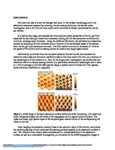
Microanalysis of Self-assembled InAs Quantum Dot Structures Grown for Infrared Detector Applications W.L. Sarney, J.W. Little, S. Svensson Sensors & Electron Devices Directorate, U.S. Army Research Laboratory AMSRL-SE-EI, 2800 Powder Mill Road, Adelphi, MD 20783 U.S.A ABSTRACT In an effort to develop materials that are sensitive to mid and far infrared radiation, we examine InAs quantum dot/GaAs matrix multilayer structures grown by molecular beam epitaxy (MBE). Customized electrical and optical properties result from nanoscale-level manipulation of the dots’ physical dimensions. The MBE growth temperature can be set to yield dots having the desired lateral dimension; however this leads to dots of insufficient vertical height. It is therefore necessary to grow the dots in a manner that allows independent control of the lateral and vertical dimensions. In this experiment, the vertical dimension is controlled by growing the dots in a multilayer structure with GaAs matrix layers. An initial layer of InAs quantum dots was grown on top of GaAs, followed by a few seconds short growth of GaAs, and then followed by the growth of another layer of InAs dots. The GaAs laterally surrounds, but does not bury, the InAs quantum dots. When the second layer of InAs dots is grown, they tend to self-organize directly on top of the exposed first layer of dots. We then grew a third layer of dots in the same manner. This effectively results in a pseudo-single layer of dots of the desired height which is then completely buried in GaAs. The goal is to develop structures that can be integrated into high operating temperature quantum dot infrared detectors (QDIPs) that have maximum sensitivity, robustness, and portability. INTRODUCTION Battlefield situational awareness can be improved with the development of sensitive infrared detectors and focal plane arrays. These detectors must quickly detect their targets in multiple daylight and weather conditions and need to perform in cluttered environments. Important applications of infrared detectors include chemical spectroscopy, image recognition, night vision, and mine detection. At the Army Research Laboratory (ARL), we research many materials systems for infrared device applications, including quantum well infrared photodetectors (QWIPS), type-II superlattices, HgCdTe structures, and quantum dot superlattices. This paper focuses on InAs quantum dots grown into superlattices with GaAs matrices onto GaAs substrates. Quantum dots provide three-dimensional confinement of electrons, as opposed to quantum wells, which confine electrons only in the direction perpendicular to the well. In a quantum dot, intersubband transitions are induced by infrared radiation of any polarization. Quantum well structures are only sensitive to vertically polarized light. To overcome this shortcoming, each pixel of a QWIP array must be integrated with a polarization rotating structure. Quantum dot growth and characterization is challenging. It is difficult to control the dots’ size, shape, and density. Since the
Data Loading...