Microstructural Evolution of Ba 2 Ycu 3 O 7 Superconductor by Electron Irradiation in a Transmission Electron Microscope
- PDF / 1,965,004 Bytes
- 4 Pages / 420.48 x 639 pts Page_size
- 22 Downloads / 377 Views
MICROSTRUCTURAL EVOLUTION OF Ba2 YCu 3 O7 SUPERCONDUCTOR BY ELECTRON IRRADIATION IN A TRANSMISSION ELECTRON MICROSCOPE KENSUKE SHIRAISHI AND HIROSHI ITOH Takasaki Radiation Chemistry Research Establishment, Japan Atomic Energy Research Institute, Watanuki-machi, Gunma 370-12, Japan
Takasaki,
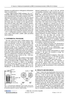
ABSTRACT Microstructural changes in a Ba2 YCu3O7 pellet were continuously observed during electron irradiation in a transmission electron microscope operating at 200 kV. Twin lamellae of 2-10 nm in thickness with 1"--50 nm spacings were seen parallel to the lattice image of (001) plane with 1.17 nm in lattice spacing. The tip of the twin was lenticular and the (001) lattice fringes were distorted around the tip. Upon intense electron beam illumination, the lamellae faded at the tip and the thickness gradually decreased which increased the spacing in the high density region. Defect clusters of about 10 nm in size were produced in the very early stage of electron illumination. INTRODUCTION The critical current density in a sintered Ba2 YCu 3 O7 pellet has been reported to be increased by irradiation with 3 MeV electrons at about 370 K[11. The radiation effect on the superconducting property can be understood by in-situ observations of the microstructure during the irradiation. The microstructural change induced by electron irradiation in crystalline Ba2 YCu 3 O7 has been observed by transmission electron microscopy[2-7]. The movement of twin boundaries was observed under an intense electron beam having an energy of 120 and 146.5 keV[2,3]. After prolonged exposure under the electron beam, the twins disappeared indicating the transformation from the orthorhombic to the tetragonal phase[2-4]. However, the twin planes in thicker regions of the crystal persisted even after 10 minutes irradiation with intense 400 keV electrons, while the twins in thin edges disappeared after 1 minute exposure to the electron beam[5]. The electron irradiation is also reported to increase distortion of the crystal about an axis parallel to the electron beam[6]. Furthermore, disordering of BaO and Y layers was induced by 0.4 and 1 MeV electron irradiations and the radiation damage took place in almost the same way in both the irradiations[7J. In addition, an amorphous phase was induced by 1 MeV electron irradiation to - 2 x 10²⁰ m-2 at 35 K18]. This paper describes the results of observations of microstructural changes in ceramic Ba2 YCu 3 O,-, during in-situ electron irradiation in a transmission electron microscope. Discussion will be made in relation to enhancement of the critical current density by electron and ion irradiations. EXPERIMENTAL A bulk sample of Ba2 YCu 3 O,- 7 was produced using standard powder metallurgy technique[l]. The specimens for transmission electron microscopy were prepared either by ion milling or by crushing the sintered pellet. The dimpled thin disk was milled at room temperature to perforation using 3 keV Ar incident on both the surfaces at an angle of 10* . The crushed crystals were suspended in ethanol, and then picked u
Data Loading...