Microstructural Evolution of Cu/Solder/Cu Pillar-Type Structures with Different Diffusion Barriers
- PDF / 4,644,717 Bytes
- 10 Pages / 593.972 x 792 pts Page_size
- 104 Downloads / 316 Views
THE Cu/solder/Cu sandwich-type structure has been extensively studied over a long period of time because it is the most common bonding structure in microelectronic packaging.[1–5] Two Cu substrates as metallizations on Si chips (or printed circuit boards) were joined with each other using solder to form an electrical connection. Conventionally, the Pb-Sn alloys, usually eutectic Pb-Sn, were used as the solder; however, they were extensively replaced by Pb-free solders in the past decades due to the concerns of Pb toxicity.[6,7] One of the promising Pb-free solders is the near-eutectic Sn-Ag alloy with a Ag content of 3.5 wt pct. Besides, the Sn-Ag alloy with a low content of hard Ag was also investigated in order to fabricate a more ductile solder joint.[8,9] Considering that Cu has high reactivity with Sn-based solder at elevated temperatures, a Ni diffusion barrier layer is usually deposited on the Cu surface to prevent HSI-KUEI/CHENG, Ph.D. Student, and TZENG-FENG LIU, Professor, are with the Department of Materials Science and Engineering, National Chiao Tung University, Hsinchu, 300, Taiwan. Contact e-mail: [email protected], [email protected], tfl[email protected] YU-JIE-LIN, Ph.D. Student, and CHIH-MING CHEN, Professor, are with the Department of Chemical Engineering, National Chung Hsing University, Taichung, 402, Taiwan. KUO-CHIO LIU, Director, is with the Backend Operation Division, Taiwan Semiconductor Manufacturing Company Ltd., Hsinchu, Taiwan. YING-LANG WANG, Professor, is with the Institute of Lighting and Energy Photonics, National Chiao Tung University, Hsinchu, 300, Taiwan. Manuscript submitted October 27, 2015. Article published online June 8, 2016 METALLURGICAL AND MATERIALS TRANSACTIONS A
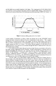
direct contact between Cu and Sn.[10,11] Interaction between Ni and Sn occurs instead of the Cu/Sn reaction and generates the Ni3Sn4 intermetallic compound (IMC) at the contact interface. The Ni3Sn4 phase grows at a slower rate than the Cu6Sn5 (and Cu3Sn) IMC that resulted from the Cu/Sn reaction, which is beneficial for the mechanical property of solder joints because a thick IMC may embrittle the bonding structure. The Cu/Ni/solder/Ni/Cu bonding structure is generally workable and reliable as a solder joint configuration for conventional packaging requirements. However, this bonding structure may suffer new challenges when applied in advanced three-dimensional (3D) integrated-circuit interconnection. In the 3D integrated-circuit interconnection, the Cu metallizations are thickened to form pillars to alleviate the electromigration impact and enhance the thermal and electrical conductivities.[12,13] Considering the standoff height requirement of solder joint, the solder volume is remarkably reduced. However, reduction of solder volume makes the solder being exhausted rapidly by the solder/Ni interaction and transformed into the IMCs. Li et al. found that complete transformation of Sn into Ni3Sn4 in a Ni/ Sn(5 lm)/Ni sandwich-type structure accompanied the joint height reduction and void formation within the Ni3Sn4
Data Loading...