Microstructure of highly p-type doped GaN sub-contact layers for low-resistivity contacts
- PDF / 1,241,444 Bytes
- 5 Pages / 612 x 792 pts (letter) Page_size
- 97 Downloads / 269 Views
E8.10.1
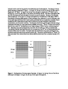
Microstructure of highly p-type doped GaN sub-contact layers for low-resistivity contacts R. Kröger, J. Dennemarck, T. Böttcher, S. Figge, and D. Hommel Institute of Solid State Physics, University of Bremen, P.O. Box 330440, 28334 Bremen, Germany ABSTRACT The effect of a highly Mg doped subcontact layer on top of GaN grown by metal organic vapor phase epitaxy and its interface to a Pd/Au contact layer was investigated by means of transmission electron microscopy and electrical characterization techniques. Use was made of prior investigations of the Mg doping characteristics, which showed the existence of a segregation related defect free layer even for doping levels as high as 5x10-19cm-3, which thickness depends on the Mg to Ga molar precursor flow ratio. For a given subcontact layer thickness of 15 nm a critical precursor molar flow ratio of 0.035 resulted in a smooth surface showing an interfacial layer indicating a Pd/Ga alloying. This layer resulted in a contact resistivity as low as 2x10⁻⁵ Ωcm2. For a flow ratio of 0.070 the surface was found to be rough due to defect formation resulting in a contact resistivity as high as 10-3 Ωcm2 similar to the value obtained without subcontact layer. Moreover, the metallization layer showed in all cases a texture of the {111} lattice planes with respect to the {0002} planes of the GaN. INTRODUCTION The realization of a sufficiently good contact to p-type doped GaN grown by metal organic vapor phase epitaxy (MOVPE) is of great importance for devices, which in many cases require current densities up to several kAcm-2 [1]. This can be realized by using highly doped Mg:InGaN or GaN:Mg subcontact layers, which provide a substantially reduced contact resistance [2,3]. Since Mg is up to now the most effective p-type dopant material an improvement of the contact resistance requires an Mg incorporation of more than 1019 cm-3 due to the fact that only 1 % of the Mg atoms contribute to the hole concentration. This objective is hampered by the formation of pyramidal defects [4,5] for such high concentrations. In prior investigations [6,7] Mg was found to segregate significantly during MOVPE growth. It could be shown that as an effect of the segregation a defect free layer can be observed even for high Mg concentrations at which a high density of pyramidal defects is created. As a simple model calculation showed the thickness of this layer depends on the molar flow ratio of the Mg and the Ga precursors. The defect free layer thickness increases drastically below a flow ratio value f of 0.020. However, at f = 0.035 the defect free layer thickness should be about 20 nm whereas it decreases to less than 10 nm for f = 0.070. Based on these predictions subcontact layers were grown for flow ratio values of 0.035 and 0.070 with both having a thickness of 15 nm to study the electrical and microstructural variations.
E8.10.2
EXPERIMENTAL DETAILS The studied samples were deposited by MOVPE and as template stacks of 200 nm undoped GaN with 1 µm thick Mg doped GaN on top was grown on
Data Loading...


