Modification of the electrical and optical Properties of Single Crystal Diamond with Focused MeV Ion Beams
- PDF / 222,117 Bytes
- 6 Pages / 612 x 792 pts (letter) Page_size
- 88 Downloads / 376 Views
1203-J17-06
Modification of the electrical and optical properties of single crystal diamond with focused MeV ion beams E. Vittone1, O. Budnyk1, A. Lo Giudice1, P.Olivero1, F. Picollo1 , Hao Wang1, F. Bosia2, S. Calusi3, L. Giuntini3, M. Massi3, S. Lagomarsino4, S. Sciortino4, G. Amato5, F. Belotti5, S. Borini5, M. Jaksic6, Ž. Pastuović,6, N. Skukan6, M. Vannoni7 , 1
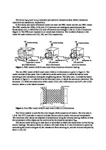
Experimental Physics Department / Centre of Excellence “Nanostructured Interfaces and Surfaces”, University of Torino, and INFN sez. Torino Via P. Giuria 1, 10125 Torino, Italy 2 Department of Theoretical Physics, University of Torino, and INFN sez. Torino, Italy 3 Department of Physics, University of Firenze and INFN sez. Firenze, , Italy 4 Department of Energetics, University of Firenze and INFN sez. Firenze, , Italy 5 Quantum Research Laboratory, Istituto Nazionale di Ricerca Metrologica, Torino, Italy 6 Laboratory for Ion Beam Interactions, Ruñer Bošković Institute, Zagreb, Croatia 7 CNR Istituto Nazionale di Ottica Applicata (INOA), Firenze, Italy ABSTRACT In this paper an overview is given on recent results obtained in the framework of an Italian/Croatian collaboration aimed to explore the potential of techniques based on focused MeV ion beams to locally modify the structural, electrical and optical features of diamond. Experiments were carried out using light (H, He, C) ion beams with energies of the order of MeV, focused to micrometer-size spot and raster scanned onto the surface of monocrystalline (IIa or Ib) diamond samples. Different energies, ion species and fluences were used, in conjunction with variable thickness masks and post annealing processes, to define threedimensional structures in diamond, whose electrical/optical/structural properties have been suitably characterized. Finite element numerical methods have been employed in the modeling of the material modification and in device design. INTRODUCTION The extreme properties of diamond make this material appealing for many applications, ranging from ionizing radiation detectors to bio-sensors, from optical and photonic devices to micro-fluidic and electromechanical systems [1]. The full exploitation of the vast potential of this material requires a fine modification of the structural, optical and electrical properties of synthetic diamond single crystals, which represent the ideal substrates in terms of material quality and reproducibility. The use of MeV ions represents one effective approach to achieve this goal [2], since the damage induced by ion beam irradiation enables the modification of the physical properties of diamond with high spatial resolution, both in depth (by tuning the end-of-range damage profile with sub-micrometer accuracy using different ion species and energies) and in the lateral directions (by focusing the ion beams down to micrometer-sized spots). A high control on the induced damage density is achieved by careful monitoring of the implantation fluence. At high damage levels, the conversion to a graphite-like phase allows the definition of electrically conduc
Data Loading...