Multilayer Precursor Synthesis of New Copper-Tungsten Selenides
- PDF / 966,798 Bytes
- 5 Pages / 414.72 x 648 pts Page_size
- 80 Downloads / 325 Views
Thick layers 4-I
LJ
0
10 20 30 40
50 60 70 80
Angle (2e)
0
10 20 30 40 50 60 70 80
Angle (20)
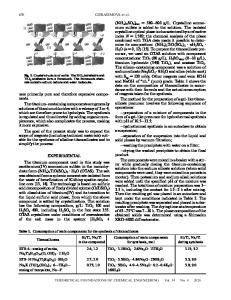
Figure 1: X-ray diffraction data contrasting the evolution of samples with 130A and 34A multilayer layer thicknesses. The data for the thick-layer sample shows the 002, 004, 006 and 008 peaks of WSe 2 after annealing at 600*C. The data for the thin-layer sample after annealing at 375*C, 540°C and 920*C is given, offset for clarity. The broad background is due to the glass support. The crystalline compound which forms at high temperatures has not yet been indexed. monitors. Samples are deposited simultaneously on silicon wafers and on photoresist-coated wafers. The samples on the coated wafers are removed from the wafer by dissolving the photoresist in acetone. The samples are then filtered and dried to give free standing samples. The multilayer layer thickness is determined by low angle x-ray diffraction, which is also used to monitor the interdiffusion of the elements. The samples are reacted in a differential scanning calorimeter to follow reactions as heat is generated either by interdiffusion or crystallization. High angle x-ray diffraction is used to determine which crystalline compounds form. Electron microscopy is performed on a Phillips CM-12 analytical TEM. Convergent beam diffraction (CBED) is obtained by reducing the spot size until the beam can be focused onto a single crystallite. Electron microscope samples are prepared by collecting a single flake of the unreacted sample on a folding TEM grid. Samples are then annealed on the grid under the same conditions as the x-ray portions of the samples.
RESULTS AND DISCUSSION In order to determine if this method can be applied in the Cu-W-Se system, a number of binary multilayers were prepared with varying layer thicknesses. The results were then used to direct the choice of layer thickness in ternary samples. Figure 1 contrasts the thermal evolution of a sample with thick layers (130A) with a sample with thin layers (34A). After annealing at 600'C, the x-ray diffraction of the thick-layer sample shows the formation of WSe 2 . The diffraction of the thin-layer sample is shown after annealing at 375°C, 540°C, and 920°C. This sample was amorphous after low temperature annealing and formed a new compound between 500°C and 900'C, without ever forming WSe 2 . This new phase has a large unit cell with many overlapping peaks. A small peak near 3° (not visible in the figure) corresponds to a d-spacing of 24A. By keeping the layer thickness below this thinner value, the formation of WSe 2 can be avoided and new phases can be formed. This behavior is 52
similar to that already seen in the Mo-Se binary system[5]. To explore this new compound, a series of thin samples were prepared, having a constant Cu-W ratio and varying amounts of selenium. A piece of each sample was mounted on a electron microscope grid to allow parallel x-ray and electron diffraction studies. These samples were found to be poorly crystallized after heating to 900'C. Between 900'C and 1000 0 C, th
Data Loading...


