Multilevel Damascene Interconnection in Integration of MOCVD Cu and Low-k Fluorinated Amorphous Carbon
- PDF / 2,298,290 Bytes
- 6 Pages / 417.6 x 639 pts Page_size
- 74 Downloads / 295 Views
challenging even though a single level structure could be easily fabricated. In this paper, we present studies on the integration process of CVD Cu with low-k fluorinated amorphous carbon (a-F:C) in single level and multilevel damascene structure. It has been shown previously that highly crosslinked a-F:C films (k - 2.5) with better thermal stability can be obtained from high-temperature PECVD deposition and thermal treatment [1-9]. However, the adhesion of a-F:C with SiO 2 and Si 3N4 is very poor. We found that a thin layer of promoter material, SiC:H, can be utilized to enhance the adhesion and mechanical property. Such a promoter layer may also serve as the barrier to contain fluorine atoms from diffusion. Using SiC:H layers, the stability and strength of Cu/SiO 2/a-F:C damascene stacking layers can be significantly improved and the structure can sustain the process of CMP, heat treatment, patterning and plasma etching. The fabrication of single and multi-level damascene structures is proved feasible. Some of the electrical performance data evaluated on the Cu/a-F:C damascene structure will be also presented in this paper. EXPERIMENTS The a-F:C and SiC:H films were deposited in a commercial PECVD system (OXFORD Plasmalab 100 system). As reported previously [6, 8, 9], the highly crosslinked a-F:C films can be obtained at 250 'C utilizing dual frequency RF discharge and then after post thermal 129 Mat. Res. Soc. Symp. Proc. Vol. 565 © 1999 Materials Research Society
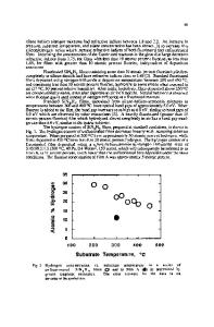
treatment. The thickness and refractive index of the a-F:C and SiC:H films were determined by a spectroscopic ellipsometer (SENTECH Instruments Gmbh). FTIR and XPS were employed to determine the bonding and chemical concentration. The isothermal test of thermal stability for the stacking layers was performed in a vacuum chamber with a base pressure of l0-5 Torr, where a deposited wafer was annealed on a heated chuck for certain period with a time fluctuation of - 2% and non-uniformity of less than 5 'C. The adhesion test is by tape pulling test and CMP. MOCVD copper was deposited using Cu-hfac-tmvs precursor with high deposition rate (2000A/min), low resistivity (- 2.tf2-cm), good adhesion, and good gap fill. Excellent adhesion of MOCVD copper film to TiN diffusion barrier film is achieved through a combination of process and equipment design [10]. The patterning of a-F:C stacking layers is by conventional plasma etching methods using 02. We use thin PECVD oxide as hardmask material to protect the a-F:C during plasma etching and resist stripping. TiN is then sputtered before copper deposition as diffusion barrier. Copper is then patterned by CMP method using commercially available system and slurry, where twostep processes are required to reduce shearing stress on surface and to prevent cracking during polishing. RESULTS AND DISCUSSION A typical one-level dual damascene structure can be displayed schematically in Figure 1, where Cu is filled in both via and trench lines. In the via contact layer, 0.5 Wmthick of SiO 2 is used as dielectric layer. For
Data Loading...