Nd: YAG laser patterning of plasma-deposited high T c superconducting thick films
- PDF / 464,534 Bytes
- 4 Pages / 576 x 792 pts Page_size
- 7 Downloads / 356 Views
Nd: YAG laser patterning of plasma-deposited high Tc superconducting thick films Usha Varshney, B. D. Eichelberger, III, J. M. Glass, and R. J. Churchill American Research Corporation of Virginia, P.O. Box 3406, Radford, Virginia 24143-3406
A. I. Kingon Department of Materials Science Engineering, North Carolina State University, Raleigh, North Carolina 27695 (Received 3 March 1993; accepted 4 June 1993)
Advances in the development of high Tc superconducting thick film components and devices for microwave, millimeterwave, and submillimeterwave applications have led to the optimization of laser patterning techniques. Plasma-sprayed superconducting thick films of YBaCuO materials on polycrystalline alumina were laser etched using an Nd: YAG laser (A = 1.06 /u,m) in the Q-switched mode. Spatial uniformity of the surface elemental distribution of Y, Ba, Cu, and Al was observed in the underlying laser-etched area. An etch rate of 7.5 yum/scan was calculated at an optimized laser fluence of 1.8 X 10⁴ J/cm 2 for a translation rate of 2.54 cm/s, having patterning widths ranging from 5-15 /mm with a heat-affected zone of 3 /mm. An absorption length of 18.3 fim for the Nd: YAG laser was determined to be suitable for patterning thick films (20-80 /tm) for device fabrication. The results are further compared to CO 2 (A = 10.6/Am) laser etching for patterning (250 yu.m) thick films.
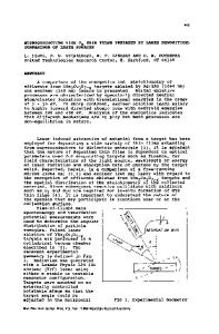
The application of plasma-spraying techniques for depositing high Tc superconducting yttrium barium copper oxide (YBaCuO) thick films has been reported by various investigators.1"11 The current work reported in this technical paper is an extension of the work published earlier on CO 2 laser patterning of plasmasprayed high Tc superconducting thick films and coatings for microwave, millimeterwave, and submillimeterwave components and devices.10'11 The significance of the laser patterning technique lies in a rapid single step dry process, as compared to the conventional lithographic procedures for device fabrication. Plasma spraying was performed using a METCO plasma flame spray system having a 9MB gun operating with a METCO type 7 MC-11 flame spray control unit in conjunction with a type 4MB powder feed unit and Model 8 MR-230 power supply with a maximum power level of 80 kW. High Tc superconducting powder received commercially from Superconductive Components Inc. (Batch No. 1124) with an average particle size of 100 /mm was plasma sprayed on 2.54 X 2.54 X 0.3175 cm polycrystalline alumina substrates. Laser etching was performed on plasma-sprayed high Tc superconducting thick films (20-80 /mm) using a Quantronix Model 117, 18 W J. Mater. Res., Vol. 8, No. 10, Oct 1993
http://journals.cambridge.org
Downloaded: 05 Apr 2015
Q-switched Nd: YAG laser (A = 1.06 /mm) operable in multimode or TEMOo- The experimental procedure has been detailed earlier.10'11 All laser-etched tracks were analyzed at the surface, as well as at the cross section, using secondary electron images on a Philips Model 505 SEM. X-ray mapping for elemental distribution over the e
Data Loading...