NH 3 Doping in MOCVD Growth of ZnO Thin Films
- PDF / 1,920,710 Bytes
- 8 Pages / 595 x 842 pts (A4) Page_size
- 115 Downloads / 525 Views
1109-B06-01
NH3 Doping in MOCVD Growth of ZnO Thin Films Tahir Zaidi1, Muhammad Jamil1, Andrew Melton1, Nola Li1, William Fenwick1, and Ian Ferguson1 1
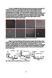
School of Electrical and Computer Engineering, Georgia Institute of Technology, Atlanta, Georgia 30332 USA ABSTRACT In this paper effects of NH3 doping on ZnO thin films grown by metal organic chemical vapor deposition (MOCVD) on c-plane sapphire substrates using diethyl zinc (DEZn) and O2 precursors and N2 as the carrier gas have been studied. NH3 flow rates were varied from 0.1% to 4% in the growth runs. All the runs were done at 500oC at 10 Torr pressure. The XRD measurements show a single ZnO (002) peak. Raman data for the samples confirms presence of ZnO:N modes at 275cm-1, 510cm-1 and 575 cm-1 and 645cm-1. The PL results for Zn rich films show weak broad peaks centered at 480nm and 650nm with no ZnO band edge emission, while oxygen rich films show weak ZnO band edge emission and a strong broad orange peak centered at 650nm. Hall effect measurements indicate that all of the as-grown films are highly resistive. Some are weakly p-type with carrier concentration of 4.24 x 1014 cm-3 and mobility of 16.55 cm2/Vs. Annealing in N2 ambient for 60 minutes at 800°C enhances the PL band edge emission and converts all the films to highly conducting ntype, with carrier concentration on the order of 8 x 1018 cm-3, mobility on the order of 12 cm2/Vs and resistivity of 0.063 Ω-cm. INTRODUCTION Zinc oxide (ZnO) with its wide bandgap (3.37 eV) and high exciton binding energy (~60 meV) is of great interest for use in optoelectronic applications. However, the major limitation it faces is the lack of reproducible p-type doping. While n-type material is easily attainable, p-type material has proved much more difficult to achieve. While several different p-type dopants and growth techniques have been reported, stability and reproducibility are still a problem. [1, 2]. Possible acceptor dopants include group-V (N, P, and As) and group-I elements (Li, Na). Out of these N substituting for O appears to be the most promising choice because of their similar atomic radii and the low activation energy of N compared to other Group V elements [3–7]. N-doped ZnO has been reported with a range of different precursors and growth techniques. MOCVD offers many advantages over other growth methods including simple and accurate doping and thickness control and scalability to production level throughput, however there are very few reports of N-doping of ZnO by MOCVD. One of the major reasons for this is the low solubility of N in ZnO, especially in a CVD process [8]. Optical properties have been studied by room temperature and low temperature photoluminescence (PL). Electrical properties of the doped ZnO thin films were studied using Hall effect measurements. Structural characteristics were determined Raman spectroscopy and X-ray diffraction (XRD). Surface morphology of the films was investigated using fieldemission scanning electron microscopy (SEM). EXPERIMENT Growth runs for undoped and N-doped Zn
Data Loading...