Nonlinear Optical Spectroscopy of Two-Dimensional WSe 2 Nanoflakes
- PDF / 1,136,639 Bytes
- 7 Pages / 432 x 648 pts Page_size
- 43 Downloads / 332 Views
MRS Advances © 2019 Materials Research Society DOI: 10.1557/adv.2019.118
Nonlinear Optical Spectroscopy of TwoDimensional WSe2 Nanoflakes Sergey Lavrov, Arseniy Buryakov, Elena Mishina, Kirill Brekhov, Nikita Ilyin, Anastasia Shestakova and Artur Avdizhiyan MIREA - Russian Technological University, 78 Vernadsky Avenue, Moscow 119454, Russia
ABSTRACT
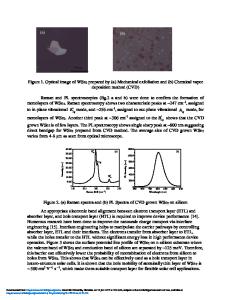
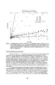
Here we present the results of the exciton states study in WSe2 and MoS2 monolayers. Thin WSe2 and MoS2 films obtained by CVD technique were studied by optical methods. The films two-dimensionality and homogeneity were confirmed by the methods of atomic force microscopy and luminescence spectroscopy. The second harmonic generation (SHG) spectroscopy technique was used for the exciton states study at room temperature in the pump photon energy range of 0.8-1.05 eV. The sevenfold SHG intensity resonance amplification was found for the 1.62 eV and 1.87 eV SHG photon energy for the WSe 2 and MoS2 films, respectively, that corresponds to the exciton transition energy. These resonance peaks belong to optical A excitons with 1s energy level.
INTRODUCTION After the discovery of graphene, active study of other various layered materials has begun. When the thickness is reduced, the optical and electrical properties of such materials may differ significantly from their bulk counterparts due to size effects. Of particular interest are transition metal dichalcogenides (TMDCs), which are twodimensional layered structures with the chemical formula MX 2, where M is a transition metal and X is a chalcogen. An important feature of this class of materials is the presence of a band gap, unlike graphene. In addition, a distinctive feature of TMDCs is an increase in the band gap with a decrease in the number of atomic layers due to the size quantization effect, which leads to a transition from an indirect-gap semiconductor in bulk material to direct-gap semiconductor in single-layered [1-3]. The width of the band gap in TMDCs monolayers is of the order of 2 eV. This makes them promising materials in the development and creation of functional elements and devices of optoelectronics, nanoelectronics and exсitonics.
Downloaded from https://www.cambridge.org/core. Cambridge University Main, on 19 Mar 2019 at 11:54:39, subject to the Cambridge Core terms of use, available at https://www.cambridge.org/core/terms. https://doi.org/10.1557/adv.2019.118
At the moment there are a number of works that demonstrate the possibility of using TMDCs in micro- and nanoelectronics devices. For example, in [4], the possibility of implementing a high-performance MoS2-based field-effect transistor was shown. The on/off ratio of this transistor was ~ 4.5×10⁷. Also, a large number of other devices are already presented: gas sensors on WS2 layers [5], high sensitivity bio sensors on WSe 2 [6] and many others. A promising joint application of TMDCs monolayers with other layered materials — graphene, black phosphorus, and silicene is also noted. For example, a structure with a MoS2 monolayer is created between tw
Data Loading...