Normal and Inverted Algan/Gan Based Piezoelectric Field effect Transistors Grown by Plasma Induced Molecular Beam Epitax
- PDF / 2,135,631 Bytes
- 6 Pages / 417.6 x 639 pts Page_size
- 53 Downloads / 251 Views
L. F. Eastmana, T. J. Eustisb, R. Dimitrovc, M. Stutzmann¢, W. Riegerd
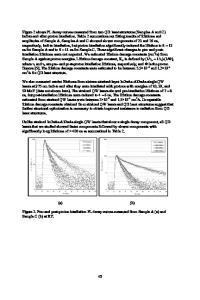
aSchool of Electrical Engineering, Cornell University, Ithaca, NY 14853 bDepartment of Materials Science, Cornell University, Ithaca, NY 14853 cWalter Schottky Institute, TU-Munich, Am Coulombwall, D-85748 Garching, Germany dFerdinand Braun Institute, Rudower Chaussee 5, D-12489 Berlin, Germany Cite this article as: MRS Internet J. Nitride Semicond. Res. 4S1, G8.4(1999) ABSTRACT High quality Ga-face and N-face AIGaN/GaN based heterostructures have been grown by plasma induced molecular beam epitaxy. By using Ga-face material we are able to fabricate conventional heterojunction field effect transistors. Because the N-face material confines electrons at a different heterojunction, the resulting transistors are called inverted. The Ga-face structures use a high temperature AIN nucleation layer to establish the polarity. Structures from these materials, relying only on polarization induced interface charge effects to create the two-dimensional electron gases, are used to confirm the polarity of the material as well as test the electrical properties of the layers. The resulting sheet concentrations of the two dimensional electron gases agree very well with the piezoelectric theory for this materials system. Hall mobilities of the two-dimensional gases for the N-face structures are as high as 1150 cm 2/Vs and 3440 cm 2/Vs for 300 K and 77 K respectively, while the Ga-face structures yield room temperature mobilities of 1190 cm 2/Vs. Both structures were then fabricated into transistors and characterized. The inverted transistors, which were fabricated from the N-face material, yielded a maximum transconductance of 130 mS/mm and a current density of 905 mA/mm. Microwave measurements gave an ft of 7 GHz and an fmax of 12 GHz for a gate length of I rtm.The normal transistors, fabricated from the Ga-face material, produced a maximum transconductance of 247 mS/mm and a current density of 938 mA/mm. Microwave measurements gave an ft of 50 GHz and an fma\ of 97 GHz for a gate length of 0.25 ptm. This shows that using plasma induced molecular beam epitaxy N-face and Ga(A1)-face AlGaN/GaN heterostructures can be grown with structural and electrical properties very suitable for high power field effect transistors. INTRODUCTION The polarity of group llI-nitrides is a subject that has seen much research recently.1 The fact that the material has wurtzite crystal symmetry means that there exists a polarity in the growth direction, yielding either Ga-face (0001) or N-face (0001) material. This polarity issue has several important consequences, some of which are the differing materials properties of the different polarities as well as how the different polarities can be achieved from a growth point of view. The polarity also determines the orientation of the spontaneous and piezoelectric G 8.4
Mat Res. Soc. Symp. Proc. Vol. 537 © 1999 Materials Research Society
polarization inside the material, which has drastic effects on device design. The devices under study a
Data Loading...