Novel fabrication method of ZnO films utilizing solid-phase crystallized seed layers
- PDF / 257,861 Bytes
- 6 Pages / 432 x 648 pts Page_size
- 35 Downloads / 265 Views
Novel fabrication method of ZnO films utilizing solid-phase crystallized seed layers Naho Itagaki and Kazunari Kuwahara Graduate School of Information Science and Electrical Engineering, Kyushu University, 744 Motooka, Nishi-ku, Fukuoka 819-0395, Japan
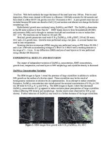
ABSTRACT A novel fabrication method of ZnO films utilizing solid-phase crystallized seed layers has been developed. In this method, solid phase crystallization (SPC) is performed by annealing amorphous ZnON films, which are prepared by sputtering of ZnO targets in Ar/N2 mixed gases, in an oxidization atmosphere. The grain size of ZnO films deposited on the seed layers is significant larger than that of ZnO films directly deposited on glass substrates, which is considered to be due to the low grain density of seed layers. By utilizing this technique, the resistivity of ZnO:Al (AZO) films is decreased from 20 × 10-4 Ω cm to 5 × 10⁻⁴ Ω cm at the film thickness of 30nm. Furthermore, we observed that SPC seed layers are in-plane aligned when Al2O3 substrates are used, which suggests that the fabrication method proposed here is also promising for synthesizing epitaxial ZnO films. INTRODUCTION Oxide semiconductors have attracted a great deal of attention not only for transparency but also for wide-ranging conductivity, which enable us to make high-performance electronic devices [1,2]. Zinc oxide (ZnO) is one of the most fascinating oxide semiconductors with unique features and a wide application range. The high electrical conductivity, the high transparency to visible lights, and the material abundance make ZnO a very promising alternative to indiumdoped tin oxide (ITO) for transparent conductive oxide (TCO). The conductivity of ZnO films, however, is lower than that of ITO, especially when the film thickness is less than 100nm, which is mainly due to the deterioration of crystallinity with decreasing the film thickness [3,4]. Meanwhile, for realization of ZnO light emitting diode (LED) and laser diode (LD), highly crystallized films with very low defect density are crucial because the defects act as nonradiative recombination centers and suppress the UV emission. To reduce the defect density, the crystal orientation needs to be well aligned since the symmetry in the crystal structure of ZnO (wurtzite, hexagonal) is low compared with that of ITO (bixbyite, cubic). Solid-phase crystallization (SPC) from amorphous phase is a promising way to fabricate the films with high crystallinity and fewer defects, which has already been used to fabricate polycrystalline silicon [5], indium oxide [6,7], ITO [8,9], and so on. However, this method has not been applied to the fabrication of ZnO films since the amorphous phase is difficult to be obtained, especially, when a sputtering method is employed for film deposition, where the high energy of impingement of sputtered species cause the nucleation. Recently, we have succeeded in SPC by sputtering deposition of amorphous zinc oxynitride (ZnON) films and subsequent
15
annealing under adequate conditions [10, 11]. The resultant ZnO films
Data Loading...