Novel TEM sample preparation using XeF 2 selective Etching
- PDF / 235,331 Bytes
- 5 Pages / 432 x 648 pts Page_size
- 11 Downloads / 488 Views
Novel TEM sample preparation using XeF2 selective Etching Ambrosini, Stefano Filo1,2, Bowen, Leon1, Mendis, Budhika1, Cirlin, George2, Bouravleuv, Alexey2, Gallant, Andrew1, Petty, Michael1, Dubrovskii, Vladimir2, Zeze, Dagou1 1 2
Durham University, Durham, United Kingdom St. Petersburg Academic University, St. Petersburg, Russian Federation
ABSTRACT We present a new approach to prepare Transmission Electron Microscopy (TEM) nanowire (NW) samples that addresses the core drawbacks of conventional techniques, which are based on mechanical polishing. The proposed method is time efficient and uses XeF2 isotropic and selective dry etching of Si to remove the host substrate from the NWs, after their embedding into a poly(methyl-methacrylate) (PMMA) matrix. Scanning electron microscopy (SEM) data suggest that NWs were grown through the gaps between the parasitic layer islands and that the stems are in direct contact with the Si substrate. This technique does not adversely affect the NWs and offers a convenient means of transferring the GaAs NWs onto other surfaces for post-process TEM analysis. It also offers excellent potential to facilitate their integration into device fabrication via a bottom-up approach, using the PMMA layer as a transfer medium.
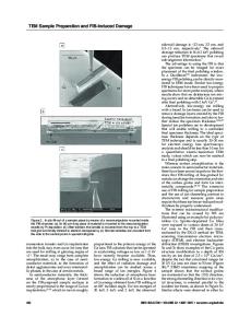
INTRODUCTION Cross sectional TEM sample preparation and analysis are critical to gain a better insight into the interaction between NWs and their substrate. Conventional TEM sample preparation involves several manual mechanical steps to reduce the thickness of the specimen until it becomes electron-transparent (below 100 nm). Mechanical grinding is very delicate, particularly as the sample becomes very thin, with the final few microns thinned down by precision ion polishing. These steps are time consuming and have a high risk of damaging the specimen [1]. The extreme fragility and critical manual handling required for such processes are coupled with intrinsic drawbacks, e.g. potential for an irreversible surface damage induced in earlier polishing steps, which are often too aggressive. Conventional solutions may include sputtering SiO2 onto the NW/Si substrate to tentatively prevent damage to the NWs [2] or focused ion beam (FIB) lamella lift-out. The latter isolates a 2x1 μm substrate slice containing NWs subsequently milled down to electron transparency by means of Ga ion beam [3]. Long process time and potential damage to the NWs by sputtering or Ga ion implantation are the main common drawbacks to both approaches. We present a TEM sample preparation method that overcomes the main drawbacks of conventional techniques. The method, based on XeF2 dry etching of silicon, is shorter in time without introducing new drawbacks. It relies on a highly efficient, isotropic and selective XeF2 etching of Si, without adversely affecting the NWs. A PMMA layer is dropcast on the front side of the Si substrate hosting the NWs to facilitate their handling and recovery. Selective and isotropic XeF2 etching of the Si backside is performed until the entire substrate is etched away, leaving
Data Loading...