Ohmic contact formation to heavily boron-doped p+ diamond prepared by hot-filament chemical vapor deposition
- PDF / 694,206 Bytes
- 7 Pages / 612 x 792 pts (letter) Page_size
- 29 Downloads / 354 Views
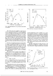
Ohmic contact formation to heavily boron-doped p+ diamond prepared by hot-filament chemical vapor deposition Shinya Ohmagari, Takeshi Matsumoto, Hitoshi Umezawa, and Yoshiaki Mokuno Advanced Power Electronics Research Center (ADPERC), National Institute of Advanced Industrial Science and Technology (AIST), 1-8-31 Midorigaoka, Ikeda, Osaka 563-8577, Japan. ABSTRACT Diamond-based rectifiers are promising devices for the development of next-generation power electronics. However, presented device structures limit current operation as low as tens A, which hampers diamond from real industrial applications. One of the critical issues is poor availability of conductive (low-resistivity) substrates which can be used for vertical-type devices for high-output operations. Recently, we have successfully fabricated heavily boron-doped (p+) low-resistivity diamond by hot-filament chemical vapor deposition (HFCVD). Resistivity was monotonically decreased to 1.2 mcm with amount of doped boron. In this study, to further investigate potentials for electric applications, contact resistance between metal/p+ diamond was evaluated by transmission line model (TLM). From the current-voltage characteristics, low specific contact resistance of ~107 cm2 was demonstrated. INTRODUCTION Diamond is attractive for high-power, low-loss, and high-temperature power devices operable under harsh environments. So far, diamond-based devices have demonstrated high blocking voltage (> 10 kV),[1] high-temperature durability (973 K),[2] and fast-switching (15 ns) characteristics.[3] It has been also reported the diodes showing high current density of more than 1 kA/cm2.[4][5] However, the actual operation current is less than tens A,[6][7] which limits the usage of diamond in industrial applications. One of the critical issues is poor availability of low-resistivity diamond substrates.[8] Heavily boron-doped p+ substrates fabricated via highpressure high-temperature (HPHT) gradient method possess relatively high resistivity,[9] which restrict the high-current operation. Also, crystalline defects existing in p+ substrates are another concern;[10] these propagate from substrate to epitaxial drift layers and cause large leakage current in blocking operation.[11] Formation of high-quality low-resistive substrates is indispensable for developing high-output diamond rectifiers. Chemical vapor deposition (CVD) have been widely used for high-quality diamond growth.[12] Among them, the microwave plasma-enhanced (MP) CVD is well adapted to grow high-purity diamond films even for low-resistivity.[13] As for the p+ substrates growth, heavily boron-doping with realistic growth rate (e.g. 110 m/h) is required to obtain freestanding plates, however, it has been pointed out that doping efficiency from CVD gas phase to diamond is very low, which limits resistivity.[14][15] The device parasitic resistance should be minimized as low as possible, i.e. less than 5% of diode's on-resistance, therefore, the target substrate resistivity of
Data Loading...