On the Nature of Weak Spots in High-k Layers Submitted to Anneals
- PDF / 287,362 Bytes
- 6 Pages / 612 x 792 pts (letter) Page_size
- 97 Downloads / 385 Views
D6.10.1
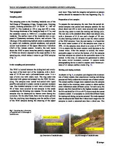
On the Nature of Weak Spots in High-k Layers Submitted to Anneals J.Pétry*, W.Vandervorst*, O.Richard, T.Conard, P.DeWolf1), V.Kaushik2), A.Delabie, S.Van Elshocht IMEC, 75 Kapeldreef, 3001 Heverlee, Belgium *also KULeuven, INSYS, Kasteelpark Arenberg, 3001 Heverlee, Belgium 1) VEECO Instruments, 11 - BP 43 rue Marie Poussepin,91412 Dourdan, France 2) Motorola Inc., 75 Kapeldreef, 3001 Heverlee, Belgium ABSTRACT In the path to the introduction of high-k dielectric into IC components, a large number of challenges have still to be solved. Some of the major issues concern the low mobility of carriers and the reliability of the devices. Trapped charges in the stack have been identified as being the cause of these issues. With this in mind, we used Conducting Atomic Force Microscopy, combined with physical analysis to understand the nature of these charges. In this contribution, we have studied the uniformity of thin HfO2 layers, with and without anneal. The Conducting Atomic Force microscopy measurements show spots of higher conductivity. Recording local IV’s in those ‘weak’ spots suggests that they consist of positive charge. On the other hand, XPS and ToFSIMS analysis show a diffusion of the interfacial SiO2 upwards into the high-k layer. Finally, the comparison of samples with differing high-k material and crystallinity indicates a strong correlation between the weak spots and the presence of silicon in the film. INTRODUCTION On the way to the sub-1 nm EOT, new materials are introduced as gate oxide to replace the SiO2. As those materials have a higher k-value their physical thickness can be kept larger while still providing the same EOT. Their enlarged physical thickness should ensure lower leakage current. HfO2 was retained among many candidates because of its high k value (k = 1825) [1] and subsequently substantial effort has been made to characterize HfO2. Many studies agree in pointing to the traps in the layer as one of the main issues regarding the HfO2 integration [2]. Identifying the defects that could be at the origin of these traps is one of the main challenges offered by the HfO2. In such a study the Conducting Atomic Force microscope (C-AFM) is of great interest as it has a nm resolution and is sensitive to microscopic electrical deficiencies. Basically, a C-AFM is an AFM with a conductive tip such that when a voltage is applied between the sample and the tip, current can flow through the sample. As the current flowing through the dielectric layer is strongly dependent on the film properties, trapped charges and leakage paths, recording the current from point to point on a scan zone, gives an overview of the electrical properties of the layer at a nanometer scale. In a previous work, we have highlighted the presence of spots of higher conductivity in annealed HfO2/SiO2 stacks [3]. The diameter of those spots, called weak spots, is on the order of 10-50 nm and their density on the order of 1010-1011 /cm2. The local increase in conductivity can have different origins: nano-crystallisation, local c
Data Loading...