Optical and Electrical Properties of Heavily Carbon-Doped Gaas Fabricated by High-Energy Ion-Implantation
- PDF / 479,954 Bytes
- 6 Pages / 414.72 x 648 pts Page_size
- 103 Downloads / 379 Views
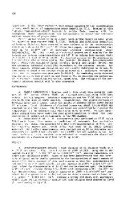
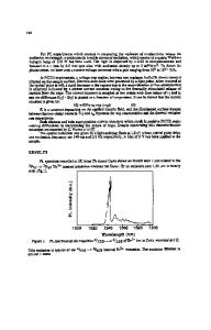
depth direction and [C] was varied in the range of lx10 19 - lx102 2 cm- 3 [5]. For dual implantation, 400 keV Ga+ ions with doses of l.4x10 13 , 1.4x10 14 and 1.4x10 15 cm- 2 were successively implanted into GaAs samples which were already implanted by 80 keV C+ ions with doses of 2.2x101 3 , 2.2x10 14 and 2.2x10 15 cm"2 , respectively. Doses and acceleration energies for dual implantation were chosen to match the depth profile of Ga with that of C. Calculated [C] 19 18 at its maximum in the depth profile, corresponding to the above each dose are 1x10 , 1x10 and 1x10 2 0 cm- 3 , respectively. Samples were furnace-annealed (FA) at 850 'C for 20 min in H2/Ar forming gas ambient and were set face-to-face with another LEC GaAs substrates during FA to minimize As desorption from the sample. For the characterization of samples, PL measurements were carried out at 2 K using the 514.5 nm line of an A"+ ion laser and 1-m monochromator. A Peltier-cooled GaAs photomultiplier and a liquid N2-cooled Ge p-i-n photodiode were used for the light detection of 800-870 nm and 800-1200 nm, respectively. Net hole concentration (INA-NDI) was obtained by using a standard van der Pauw technique at RT. RESULTS AND DISCUSSION Figure 1(a) shows the 2 K PL spectra of C+ ion-implanted samples as a function of [C], obtained by GaAs detector. Figure l(b) indicates the PL spectrum for [C]=lxl0 22 cm-3, obtained by Ge detector. PL spectra for a starting un-implanted substrate and that of simply annealed one are also shown. Transition from conduction band to C acceptors, (e, C) located at 830 nm is the predominant emission for un-implanted GaAs. Recombination at unidentified donor - C acceptor pairs, (D, C) is found at 832 nm. The C-related emissions, (e, C) and (D, C) in un-implanted
GaAs suggest that C is the principal residual impurity in LEC GaAs substrate. Close to GaAs band-edge, emissions due to free excitons, (F.E.) and excitons bound at neutral C acceptors, (C', X) are observed at 1.516 eV and 1.513 eV,
PHOTON EoNERCY (eV)
>.
De--o
b
-
Furnace Annealed
-
C-GaAs
u
respectively. For C+ ion-implanted samples with . [C] up to 5x10 2
1
c,
cm- 3 , no specifically new
cc1.x1022 cm-,)
...0.00
emission is identified and moreover the emission
1100
1....1 2 H lON (a)Ga.s Detetor
E.1aY
ground-state acceptor atoms appears for [C]=lxl0 1 7 - 5x10 1 8 cm- 3 [10]. Even when comparably heavy-mass ions such as Cd+ or Hg+ ions are implanted into LEC GaAs and heat-treated
796
4
0 '.n
(c].In 1 ' (cm.)
LEG GaAs (Annealed) FEc.,x)/*•
wafers describe that by FA treatment, the emission soo . 0 assigned as [g-g], attributed to the pairs between
IeV
-.
optically well activated. Our previous works on
high-energy (400 keV) C+ ion-implantation into molecular beam epitaxy (MBE)-grown GaAs
0
(n,) WAVELENGTH
intensity quenches steeply with increasing [C].
It has been repeatedly demonstrated that for INA-NDI>--lxl 10 7 cm- 3 , C-doped GaAs exhibits unexceptionally multiple acceptor-acceptor pair emissions such as "g", [g-g], [g-g]ax and
Data Loading...


