Optical and Microstructural Characterization of Nanocrystalline Silicon Superlattices
- PDF / 1,450,947 Bytes
- 13 Pages / 417.6 x 639 pts Page_size
- 92 Downloads / 401 Views
INTRODUCTION The current world-wide interest in nanocrystalline Si (nc-Si) resulted primarily from the Canham's 1990 proposal [1] that efficient visible light emission from high porosity structures arises from quantum confinement effects. This is particularly intriguing for three reasons. First, because nc-Si is a Si structure and bulk Si is spectacularly inefficient at emitting light, even at cryogenic temperatures. Second, because the light emitting nanostructure (e.g. porous Si) can be "made in a bucket" within minutes, without resort to either the costly lithographic or epitaxial techniques that were at the time, the conventional approaches to realizing exceeding small structures. Third, because Si is the most technologically important material known to mankind, dominating the microelectronics revolution that influences our everyday
173 Mat. Res. Soc. Symp. Proc. Vol. 588 ©2000 Materials Research Society
lives. The original proposal that light-emitting Si devices could eventually result in a new generation of Si chips and extend the functionality of Si technology from microelectronics into optoelectronics was exciting and encouraging. Thousands of papers and strong knowledge of the nature and properties of light emission in nanoscale Si were generated. The question is: where are we ten years on? Can nanoscale Si meet the expectations and be used in Si nano- and optoelectronics? Can a reliable device be fabricated in a research laboratory and, eventually, be transformed to a real commercial manufacturing? The price for the simplicity in porous Si fabrication is high: the structure is fragile, and the Si nanocrystal size distribution is broad. Among the many approaches to fabricate Si nanocrystals, the thermal crystallization of amorphous Si (a-Si)/Si0 2 layered structures [2] shows great potential. The Si nanocrystals are packed in the form of ordered layers, and their size and packing density can be controlled precisely. This
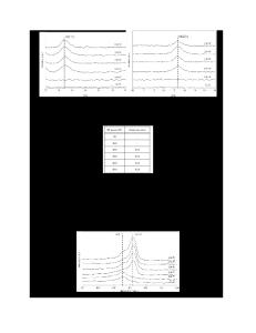
type of structure has been called a nanocrystalline Si (nc-Si) SL because it consists of periodically alternating layers of Si nanocrystals and Si0 2 . In this work we show that the nc-Si SL prepared by controlled crystallization exhibits nearly perfect nc-Si/Si0 2 interfaces and a narrow nanocrystal size distribution. We show that several techniques which have been developed and used for conventional SL characterization are applicable for nc-Si SL metrology. In addition, we discuss in detail the light emitting properties of nc-Si SLs. SAMPLE PREPARATION AND STRUCTURAL CHARACTERIZATION The magnetron sputtering of the a-Si/Si0 2 multilayers was performed at Rochester in a Perkin-Elmer 2400 sputtering system by radio-frequency (RF) sputtering and plasma oxidation. In the sputtered samples, the a-Si thickness ranged from - 20 to 250 A and that of the Si0 2 from 25 to 60 'A.The number of periods varied from 1 to 60. The crystallization was performed by rapid (40-60 s) thermal annealing (RTA) at 800900 0 C followed by furnace annealing. In the furnace annealing step, the temperature was inc
Data Loading...