Optical Properties of Controllable Self-Assembled Lateral Nanostructures on InN, InAlN, and AlN Thin Films
- PDF / 184,990 Bytes
- 6 Pages / 612 x 792 pts (letter) Page_size
- 78 Downloads / 303 Views
L11.27.1
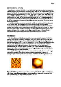
Optical Properties of Controllable Self-Assembled Lateral Nanostructures on InN, InAlN, and AlN Thin Films Yuri Danylyuk,* Dmitri Romanov,*** Eric McCullen,* Daad Haddad,** Ratna Naik,** and Gregory Auner* *Department of ECE, Wayne State University, Detroit, MI 48202, U.S.A. **Department of Physics, Wayne State University, Detroit, MI 48202, U.S.A. ***Department of Physics, Temple University, Philadelphia, PA 19122, U.S.A. ABSTRACT Utilizing plasma source molecular beam epitaxy (PSMBE), we have grown epitaxial InxAl1-xN films on (0001) sapphire substrates; the indium concentration, x, varied from 0 to 1. The atomic force microscopy of the films reveals characteristic surface patterns of nanometer scale. The feature size distribution is determined by the film composition and thickness. Both absorption and reflection spectra of the films have additional peaks below the fundamental absorption threshold. These peaks cannot be associated with N vacancies or any other known crystal defects and impurities. We attribute the peaks to electron confinement in the hillocks of the lateral structure by the strong electric field of piezoelectric and spontaneous polarization that is characteristic to nitride semiconductor compounds. The calculated values of the electron energy levels are in good agreement with the spectroscopic data; moreover, the electron confinement model explains the observed temperature dependence of the additional peaks. The hillock size control will allow one to control the optical and transport properties of the films. INTRODUCTION Ternary alloys of AlN and InN have been studied extensively in the regard of their potential application in light-emitting and laser diodes [1], primarily because of their wide direct band gap, tunable by composition and ranging from 0.7 eV for InN[2], to 6.2 eV for AlN. The devices, based on quantum wells or on self-assembled arrays of quantum dots, are expected to cover wavelength region from ultraviolet to near infrared light. Given excellent radiation and thermal stability of the materials, such devices will be especially useful in space and medical applications. However, the progress toward these goals is impeded by technological difficulties of the Al1-xInxN film growth [3-6]. These difficulties are associated with spinodal phase separation that frustrates solubility between AlN and InN [7]. Various substrates and various growth techniques have been tried to achieve reliable growth of Al1-xInxN thin films: metalorganic vapor phase epitaxy [1], magnetron reactive sputtering [3,6], metal-organic chemicalvapor deposition [4], and microwave-excited metalorganic vapor phase epitaxy [5]. The films obtained varied from spontaneously segregated polycrystalline to highly oriented epitaxial. In the present work, we have studied a series of Al1-xInxN alloy films with thickness ranging from 100 nm to 8000 nm and In concentration ranging from 0 to 1. We have identified the presence of a large number of bulges as the specific feature of the film morphology. We focused our attent
Data Loading...