Optimization of the protocrystalline p -layer in a -Si:H-based n - i - p photodiodes
- PDF / 528,463 Bytes
- 6 Pages / 595.22 x 842 pts (A4) Page_size
- 33 Downloads / 249 Views
Optimization of the protocrystalline p-layer in a-Si:H-based n-i-p photodiodes Y. Vygranenko1,2, M. Fernandes1,2, M. Vieira1,2, A. Sazonov3 1 Electronics, Telecommunications and Computer Engineering, ISEL, Lisbon, 1950-062, Portugal 2 CTS-UNINOVA, Quinta da Torre, 2829-516, Caparica, Portugal 3 Electrical and Computer Engineering, University of Waterloo, Waterloo, N2L 3G1, Canada
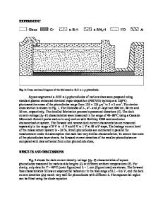
ABSTRACT This work reports a carbon-free, blue-enhanced a-Si:H n-i-p photodiode with an optimized protocrystalline p-layer. Although the used deposition conditions for the p-layer correspond to the microcrystalline regime, thin layers are mostly protocrystalline due to the amorphous underlying undoped layer. This conclusion is supported by Raman spectroscopy measurements. We have also found that the optical band gap of the p-layer can be varied by adjusting the rf power. By widening the band gap and tuning the impurity concentration in the p-layer, absorption and recombination losses at the p-i interface were reduced. The current-voltage, capacitance-voltage, and spectral-response characteristics of fabricated photodiodes are correlated with the doping level, optical band gap, and deposition conditions for p-layers. The optimized device exhibits a leakage current of about ~80 pA/cm2 at 5 V reverse bias. The external quantum efficiency reaches a peak value of 92% at a wavelength of 510 nm, and, at shorter wavelengths, decreases down to 66%@400nm. INTRODUCTION Hydrogenated amorphous silicon (a-Si:H) p-i-n photodiodes are commonly used as pixel sensors in digital radiographic flat-panel imaging detectors [1]. Photodiode performance is one of the factors limiting the signal-to-noise ratio and image quality. In particular, a high sensor sensitivity in the visible spectral range is required to provide an efficient optical coupling with conventional phosphors such as CsI:Tl or Gd2O2S:Tb [2]. One of the approaches to minimize the absorption losses in the p-layer is to use an a-Si1-xCx:H alloy having a wider band gap than a-Si:H [3-5]. However, the use of this technology in industry is limited because the most of production lines are for a-Si TFT backplanes, and the cost of their upgrade for additional doping gases may be unacceptably high. In this work, we report on a carbon-free, blue-enhanced n-i-p photodiode by incorporating p-type doped protocrystalline silicon (pc-Si:H). In earlier studies, this material was applied to a-Si:H n-i-p solar cells to improve their performance through an increase in the open circuit voltage and a reduction in the series resistance [6-8]. Specifically, the thin (~20 nm) p-layers were prepared at low temperatures (< 200 oC) by PECVD using high hydrogen-to-silane flow ratios (typically R = [H2] / [SiH4] ~ 50 - 200) without crossing the thickness-dependent transition into the mixed-phase (amorphous + microcrystalline) growth regime. The growth of such p-layers follows a thickness evolution in which pure protocrystalline material is observed at the p-i interface and a low density of nanocrystallites nucleates with incr
Data Loading...


