Opto-electrical characterization and X-ray Mapping of large-volume cadmium zinc telluride radiation detectors
- PDF / 601,472 Bytes
- 6 Pages / 612 x 792 pts (letter) Page_size
- 28 Downloads / 304 Views
1164-L10-07
Opto-electrical characterization and X-ray Mapping of large-volume cadmium zinc telluride radiation detectors
G. Yang, A. E. Bolotnikov, G. S. Camarda, Y. Cui, A. Hossain, H. W. Yao, K. Kim and R. B. James Brookhaven National Laboratory, Upton, NY 11973, U.S.A.
ABSTRACT Large-volume cadmium zinc telluride (CZT) radiation detectors would greatly improve radiation detection capabilities and, therefore, attract extensive scientific and commercial interests. CZT crystals with volumes as large as hundreds of centimeters can be achieved today due to improvements in the crystal growth technology. However, the poor performance of largevolume CZT detectors is still a challenging problem affecting the commercialization of CZT detectors and imaging arrays. We have employed Pockels effect measurements and synchrotron X-ray mapping techniques to investigate the performance-limiting factors for large-volume CZT detectors. Experimental results with the above characterization methods reveal the non-uniform distribution of internal electric field of large-volume CZT detectors, which help us to better understand the responsible mechanism for the insufficient carrier collection in large-volume CZT detectors.
INTRODUCTION Cadmium zinc telluride (CZT) has been considered a promising material for roomtemperature nuclear radiation detection, since it provides high detection-efficiency and good energy-resolution without a complicated cooling system [1-3]. Since the first practical CZT gamma-ray detector reported in 1992 [2], there have been many advances in the performance of the devices. However, most of previous investigations were focused on small-volume CZT detectors because of the limited availability of large-volume CZT single crystals. Actually largevolume CZT detectors are always desired because they substantially improve the detectionefficiency and reduce the measurement time, which are especially important in hand-held gamma-ray spectrometers, medical imaging systems and astrophysics experiments. Unfortunately, even though recent developments of crystal growth techniques provide a better availability of large-volume CZT crystals, it is still difficult to fabricate large-volume CZT detectors with high carrier collection efficiency. An important parameter that substantially affects the carrier collection efficiency and, therefore, the performance of CZT detectors, is the distribution of the internal electrical field; a uniform distribution is always desirable. However, to our knowledge, until now there are few reports to investigate the electric field distribution of large-volume CZT detectors. In this work, we employed a Pockels effect (PE) measurement system and synchrotron X-ray mapping technique to investigate the electric field distribution of a
large-volume CZT detector. To avoid the complexity introduced by different contact configurations, our research is focused on Au–CZT planar detectors, because the planar configuration of contacts is the basic one used for commercial nuclear radiation detectors. The un
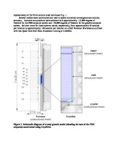
Data Loading...