Optoelectronic Characterizations of Porous Silicon
- PDF / 370,684 Bytes
- 6 Pages / 420.48 x 639 pts Page_size
- 47 Downloads / 487 Views
OPTOELECTRONIC CHARACTERIZATIONS OF POROUS SILICON
NOBUYOSHI KOSHIDA AND HIDEKI KOYAMA Tokyo University of Agriculture and Technology, Faculty of Technology, Division of Electronic and Information Engineering, Koganei, Tokyo 184, Japan
Abstract The optoelectronic properties of porous Si (PS) have been investigated in relation to the visible luminescence characteristics. First, the electronic structure has been characterized by spectroscopic ellipsometry and synchrotron orbital radiation (SOR) reflection spectra analyses. A retention of the original crystallinity, accompanied by a band gap widening, is confirmed by the optical reflection spectra and the optical constants behavior. Second, it is shown that there exists an intrinsic correlation between the visible photoluminescence characteristics of PS and its interfacial and electrical properties. These experimental results suggest that in the visible luminescence mechanism of PS, both band modification in Si crystallites and passivation at their surface play a complementary role to each other. The former ensures sufficient electronic excitation and the latter contribute to suppression of nonradiative relaxation.
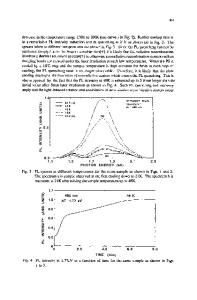
INTRODUCTION Visible photoluminescent (PL) [1-4] and electroluminescent (EL) [5,6] properties of porous silicon (PS) and its related photoelectronic properties [7,8] have shown the potential usefulness of PS as a novel optoelectronic material. The luminescence mechanism in PS, however, remains controversial. This is mainly due to the difficulty in characterizing PS which consists of a great number of complicated Si nanostructures with an extremely large specific surface area. The understanding of the origin of visible light emission from PS is required in order to establish the basis of the Si nanostructure physics and technology. In the present paper, the optical, interfacial and electrical properties of PS are characterized in relation to the visible luminescence characteristics. To avoid the effect of Si substrates, most measurements are carried out for self-supporting PS samples.
EXPERIMENTAL Sample Preparation The PS layers were formed by anodization of nondegenerate p-type Si wafers in 20-50% 2 aqueous or ethanoic HF solutions at current densities of 10-80 mA/cm for 5-60 min in the dark or under the illumination by a 500 W tungsten lamp from a distance of 20 cm. In some cases, illumination was employed after anodization. The thickness of PS layers is 3 to 50 Jim. Usually, the studies of PS are carried out under the condition that the PS iayer is not separated from the Si substrate. For optoelectronic characterization of PS, -however, it is necessary to evaluate the intrinsic nature of PS without the effects of the Si substrate. Particularly, the temperature dependence of the material, optical, electrical and luminescent characteristics should be studied for self-supporting PS samples from which stress-induced effects at the PSsubstrate interface can completely be removed. For this purpose, some self-supporting PS films were prepared by electrochem
Data Loading...