Origin of ring defects in high In content green InGaN/GaN MQW: An Ultrasonic Force Microscopy Study
- PDF / 259,697 Bytes
- 7 Pages / 612 x 792 pts (letter) Page_size
- 81 Downloads / 251 Views
Internet Journal Nitride Semiconductor Research
Origin of ring defects in high In content green InGaN/GaN MQW: An Ultrasonic Force Microscopy Study F. Shahedipour-Sandvik1, M. Jamil1, K.Topol1, J. R. Grandusky1, Kathleen A Dunn1, J. Ramer2 and V. N. Merai2 1College 2Veeco
of Nanoscale Science and Engineering, University at Albany-SUNY, Albany, NY 12203, Corp. 394 Elizabeth Avenue, Somerset, NJ 08873,
(Received Tuesday, June 21, 2005; accepted Monday, October 3, 2005)
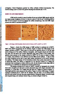
Observation of GaN-based islands surrounded by V-defects in the barrier layer of green LED is reported for InGaN MQWs deposited under no hydrogen or at growth temperatures of less than 800°C. Nanoscale mechanical properties of the areas enclosed and outside of the ring defects does not show any appreciable variation as measured by UFM. Chemical etching of the MQW structure in addition to cross-sectional TEM analysis ruled out the possibility of growth of inversion domains of N-polar GaN in a Ga-polar GaN matrix.
1
Introduction
The III-Nitride material system has been shown to possess great potential for applications which require devices with a wide spectral response, high breakdown voltage and high temperature and chemical stability. It is therefore highly desirable to understand and control the growth mechanisms of this material system at an atomic level so that one can manipulate the structural growth to achieve the desired properties. It is widely known that GaN epitaxial layers grown on non-native substrates contain high defect densities due to the thermal expansion coefficient and lattice mismatch between the layers. These defects include threading dislocations (TDs), stacking faults, and inversion domain boundaries. [1], [2] The presence of these defects affects the optical and structural quality of the InGaN/GaN multiquantum well (MQW) structures and usually results in open V-defects at the surfaces. [3], [4] Due to the high intrinsic strain between the QW layers, the physical properties of the MQW structure vary strongly over distances of a few nanometers. The resultant variation in the local elastic properties strongly affects electrical and optical properties of the material and influences the growth mechanism. It has been shown that the mismatch stress causes high dislocation densities in GaNbased devices and increases the threshold current density in stimulated emission in laser structures. [5] The formation mechanism of the so-called V-defects in InGaN/GaN based structures is not yet well understood. The study performed by Cho et al. concluded
that there are three main mechanisms for the formation of V-defects depending on the In composition of the InGaN well layer. [6] The origin of the V-shaped pits has also been attributed to threading dislocation defects and increased strain energy. [2], [3], [7], [8], [9], [10] Most of the previous studies on the origin of V-defects have been obtained from InGaN/GaN MQWs with In compositions of less than 20%, and only a few reports have presented results for higher In compositions. The diffic
Data Loading...


