P Implantation Effect on Specific Contact Resistance in 3C-SiC Grown on Si
- PDF / 169,184 Bytes
- 6 Pages / 612 x 792 pts (letter) Page_size
- 42 Downloads / 222 Views
1068-C07-09
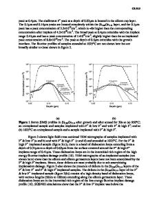
P Implantation Effect on Specific Contact Resistance in 3C-SiC Grown on Si Anne-Elisabeth Bazin1,2, Jean-François Michaud1, Marc Portail3, Thierry Chassagne4, Marcin Zielinski4, Jean-Marc Lecoq2, Emmanuel Collard2, and Daniel Alquier1 1 Laboratoire de Microélectronique de Puissance, Université François Rabelais de Tours, 16 Rue Pierre et Marie Curie, BP 7155, Tours Cedex 2, 37071, France 2 STMicroelectronics, 16 Rue Pierre et Marie Curie, BP 7155, Tours Cedex 2, 37071, France 3 Centre de Recherche sur l’Hétéro-Epitaxie et ses Applications CNRS–UPR10, Rue Bernard Grégory, Valbonne, 06560, France 4 NOVASiC, Savoie Technolac, Arche Bât 4, BP 267, Le Bourget du Lac Cedex, 73375, France ABSTRACT In this work, non-intentionally doped 3C-SiC epilayers were implanted using phosphorus at different energies and subsequently annealed at temperatures between 1100°C and 1350°C in order to form n+ implanted layers. Different techniques such as Fourier Transformed InfraRed spectroscopy (FTIR) and Secondary Ion Mass Spectroscopy (SIMS) were used to characterize implanted 3C-SiC epilayers after the different annealing steps. Successively, metal layers were sputtered in order to form the contacts. The specific contact resistance (ρC) was determined by using circular Transfer Length Method (c-TLM) patterns. Specific contact resistance values were investigated as a function of doping and contact annealing conditions and compared to those obtained for highly doped 3C-SiC epilayers. As expected, ρC value is highly sensitive to postimplantation annealing and metal contact annealing. This work demonstrates that low resistance values can be achieved using phosphorus implantation and, hence, enabling device processing. INTRODUCTION Since last decades, silicon carbide (SiC) is the subject of intensive research and development activities. This growing attention is motivated by attractive mechanical and electrical properties which make silicon carbide a promising material for high power and high temperature electronic devices. According to the stacking sequence of the Si-C bilayers, silicon carbide exists in more than 200 different polytypes. Compared to the various existing structures, the 3C-SiC is the only one that can be hetero-epitaxially grown on cheap silicon substrates. The SiC growth capability on low cost and large diameter silicon substrates becomes then a very attractive solution for manufacturing [1]. Indeed, in such conditions, only the required silicon carbide thickness has to be grown according to the targeted application. For such a material, one of the main challenges is the achievement of high quality ohmic contacts in order to create efficient electronic devices. To reach that, ohmic contacts both in highly doped epitaxial or implanted layers may be required depending on process flow. Indeed, doping is a key process in semiconductor manufacturing. Ion implantation is a method of choice to obtain selective doping and the only available for silicon carbide. To obtain n+ doping in 3C-SiC, both nitrogen and phosphor
Data Loading...