Phase Formation Sequence in the Pd-GaAs System
- PDF / 2,409,517 Bytes
- 6 Pages / 417.6 x 639 pts Page_size
- 105 Downloads / 363 Views
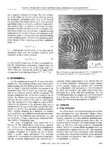
368 from polycrystalline films are not sufficient to identify phases in this system. Furthermore, the structural data from TEM studies [2,3] suggest that if phases such as PdAs 2 , Pd2 Ga and, Pd2 As are present, they account In this paper, the for only a small fraction of the film volume. compositional and morphological features of the ternary phase reactions are investigated by application of TEM and Rutherford backscattering (RBS) Emphasis is placed on the interrelationships between techniques. crystallographic texture and the nucleation and growth of phases I and II. EXPERIMENTAL METHODS Palladium films were deposited by e-gun evaporation to thicknesses Uncapped of 19-60 nm onto chemically cleaned (100) SI GaAs (undoped). and S10 2 - capped samples were annealed at temperatures up to 500'C in Both plan-view and cross-sectional TEM specimens flowing forming gas. were imaged in a top-entry JEOL JEM 200 CX at 200 keV. Compositional data were obtained from the same specimens by acquiring EDS spectra in a JEOL 200 CX TEM/STEM equipped with an ultra-thin-window x-ray detector. The concentration ratios of [Ga] to [As] were calculated using spectra from the GaAs substrate for calibration. Since reliable Pd-Ga standards are not available, the [Pd] to [Ga] ratios were estimated from the theoretical formula, [Pd]/[Ga]v = k (IPdL/IGaKa) [6], which relates the ratio of concentrations of Pd and Ga to the ratio of total counts (intensities) in the L-series of Pd and the Ks peak of Ga for a thin-foil In addition, reacted films which were shown by TEM to consist specimen. were analyzed by RBS. Measurements were performed using of a single phase both 2 MeV 4 He and 20 MeV 160 projectiles. The heavy-ion RBS (20 MeV 160) allowed the separation of the Pd signal from the substrate signal for the thicker films (60 nm Pd). RESULTS AND DISCUSSION Nucleation and growth of phase I The cross-sectional TEM micrograph in Fig. 1 reveals the thin layer Palladium is the primary of phase I which forms during deposition. In diffusing species as indicated by the position of the native oxide. this specimen the grains of phase I are -.6nm thick by 018nm wide with 100 Adjacent grains are I/GaAs and {1llO}I -- // { }GaAs. typically misoriented by 5-10. In order to determine the orientation relationship uniquely (recall that [011] and [011] are not equivalent in the (100) surface), samples
Fig. 1. Cross-sectional TEM micrograph of phase I layer formed during deposition of Pd onto (100) GaAs.
369
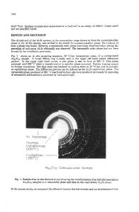
were etched in C12 :CH 3OH. Etchpits at pinholes in the Pd film displayed the characteristic rectangular projected shape with the long_-axis parallel to [01T] such that the exposed gallium planes ((lll)A and (1ll)A) intersect This information allowed along [011] at the bottom of the pit [7-9]. the unique determination of the orientation of cross-sectional TEM specimens. Diffraction patterns recorded with the electron beam parallel Grains with to [011] and [01] (Fig. 2) show that [O00l]i//[Oll]GaAs. During the reaction at higher [O001]i//[Oll]GaAs were not o
Data Loading...


