Photo-Irradiation-Induced Narrowing of Photoluminescence Spectra from Porous Silicon
- PDF / 453,861 Bytes
- 6 Pages / 414.72 x 648 pts Page_size
- 50 Downloads / 353 Views
Mat. Res. Soc. Symp. Proc. Vol. 452 ©1997 Materials Research Society
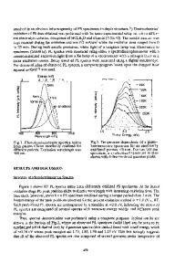
Table I Fabrication conditions used in the present study. In the columns of current density and time, numerals before and after "/" are corresponding values in the anodization process and in the photo-irradiation process, respectively. In the anodization process, no light illumination was carried out to p-type wafers whereas a tungsten lamp of 260 lx was illuminated to n-type wafers. In the photo-irradiation process, the specimen surface was illuminated to 1.7 x 10⁵ Ix using a tungsten lamp. condition
re
ty
and
resistivity (f2cm)
anodization process / current density (mA/cm 2 )
photo-irradiation process time (s)
A B C D
p(100) p(l00) p(100) p(100)
14-22 14-22 14-22 14-22
2 2/2 2/0 2/20
30, 40, 50, 60 345/15, 330/30, 315/45, 300/60 360/20, 360/30, 360/45, 360/60 345/15, 330/30, 315/45, 300/60
E F
n(100) 1.46 n(100) 1.46
2/2 2/20
340/20, 330/30, 315/45, 300/60 330/30, 315/45, 308/52, 300/60
G
n(100) 1.46
2/40
330/30, 315/45, 300/60, 285/75
minutes, and (2) subsequently anodized under photo-irradiation for dozens of seconds with anodization current flowing. 2. EXPERIMENTS P-type Si (100) wafers with a resistivity of 14 - 22 £ cm were used for experiments in 3.1 and 3.2. Ohmic contacts for the p-type wafers were formed by aluminum evaporation onto their back sides and subsequent annealing at 500 'C for 10 min in a high vacuum. For experiments in 3.3, ntype Si (100) wafers with a resistivity of 1.46 Q cm were used. Ohmic contacts of the n-type wafers were formed by annealing at 500 'C for 5 min in a high vacuum after titanium evaporation onto their back sides, and by subsequent gold evaporation onto them to prevent from oxidation. These wafers were anodized in a solution consisting of HF (47%) : C2H5OH = 1 : 1. A tungsten lamp was used for photo-irradiation when necessary. The fabricating conditions used are shown in Table I, where "anodization process" means the first stage for fabricating samples with sufficiently thick PS layers (thickness =1 gm) without photo-irradiation for the p-type Si wafers although a weak light of 260 lx was illuminated to the n-type Si wafers, while "photo-irradiation process" means the second stage for fabricating PS under photo-irradiation of 1.7 x 10⁵ Ix. PL measurements were performed using a spectrofluorophotometer with excitation of 300-nm ultraviolet light monochromatized from a Xe arc lamp of 150 W. 3. RESULTS AND DISCUSSION 3.1 Effect of Photo-irradiation Timing In order to compare the effect of photo-irradiation during the PS fabrication process on the PL spectra, PS samples were fabricated from the p-type Si wafers in the following two ways. In one
530
..
0.45............ . 60...... .......-. Cniion A 0.50
1500
--4 i ICondition ....-Condition o i o.AB
-.
`45
00
.......... --------5
0.25.....
...... *
3. 0.20 .... : "-......... ......... 3 -,....... 02..............
....
o
0ý5o
800
550
600
650
700
750
.........--------
60
600
650
700
750
800
Peak Wavelength (nm)
Data Loading...