Photoluminescence from amorphous SiO 2 /Silicon/amorphous SiO 2 single quantum well structures
- PDF / 181,842 Bytes
- 5 Pages / 595 x 842 pts (A4) Page_size
- 41 Downloads / 366 Views
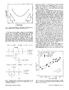
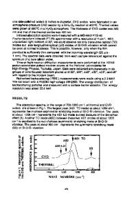
Photoluminescence from amorphous SiO2/Silicon/amorphous SiO2 single quantum well structures Y.Q. Wang, Y. Ishikawa, and N. Shibata Japan Fine Ceramics Center, 2-4-1 Mutsuno, Atsuta-ku, Nagoya, 456-8587, Japan ABSTRACT Amorphous silicon dioxide/silicon/amorphous silicon dioxide single quantum well structures were fabricated by oxygen implantation followed by thermal oxidation. No photoluminescence (PL) was observed from the as grown samples. We found that annealing in hydrogen allows the single quantum well (SQW) structures to emit twopeak (blue and yellow) PL at room temperature (RT). The blue PL (2.9 eV) does not change with the thickness of Si layers or the temperature. The yellow peak varied from 2.0 eV to 2.4 eV with thinning of the Si layer from 5 nm to 0.5 nm. Lowering the temperature also changed the yellow peak position of the 1.5 nm Si-SQW structure from 2.3 eV (RT) to 2.6 eV (8.4 K). We conclude that the blue PL is from SiO2 and the yellow PL is caused by a recombination process in the Si-SQW. INTRODUCTION The observation of visible photoluminescence (PL) from porous Si [1] has stimulated the search for its origin [2-4], as the light emitting Si makes possible the development of optoelectronic Si devices. However, the dimensional imprecision and surface instability of porous Si complicate investigation of the light emitting process. Reducing the light emission process to its simplest components should enable us to clarify the origin of the PL. Knowledge of the cause of the PL will enable the development of precisely controlled optoelectronic devices. One of the solutions is to use a Si-single quantum well (SQW) which is sandwiched between layers of SiO2, as varying the thickness of the Si will enable us to analyze its effect on the PL, and sandwiching Si between SiO2 improves the surface stability [5-11]. In the present paper, we have fabricated an Si-SQW sandwiched between SiO2 using a silicon-oninsulator (SOI) technique and thermal oxidation. Blue and yellow PL were observed at room temperature. It is found that the yellow PL shifted to blue with thinning of the Si layer, while the blue PL is stable despite the change in the Si thickness.
EXPERIMENT Si-SQW structures were created by the separation by implanted oxygen (SIMOX) technique and thermal oxidation. The starting substrate was a p-type Si (100) with resistivity of 5-10 Ω cm. Low energy oxygen ions (O+) were generated by an electron-cyclotron-resonance bucket ion source with a sector magnet. Oxygen ion implantation (25 keV) was performed at 550 oC with a current density of 130-140 µA/cm2 on Si to a dose of 2 x 1017cm-2 [12]. Ex situ annealing, which was performed at 1280 oC for 6 hours in an N2 gas flow containing 0.5% O2, creates a uniform SOI substrate [13]. Removing the top SiO2 film using diluted HF solution produces a 50
F5.18.1
nm-Si/50 nm-SiO2/Si substrate structure. Finally, Si-SQW structures were obtained by thinning the top Si layer by thermal oxidation at 800 oC in a dry oxygen flow. Transmission electron microscopy (TEM) was used fo
Data Loading...